Method and a system for producing a semi-conductor module

a semi-conductor module and semi-conductor technology, applied in the direction of individual semiconductor device testing, semiconductor/solid-state device testing/measurement, instruments, etc., can solve the problems of insufficient quantity of desired electric contact, easy error in bumping contact, complex wiring form, etc., to achieve rapid and economical changes or adaptations, and increase the cost of modules

Active Publication Date: 2015-10-20
SWISS TECH ENTERPRISE GMBH
View PDF41 Cites 3 Cited by
  • Summary
  • Abstract
  • Description
  • Claims
  • Application Information

AI Technical Summary

Benefits of technology

[0015]It is an object of the invention to provide a method and a system for producing a semi-conductor module with which the aforementioned problems are resolved, and in particular a semi-conductor module can be produced efficiently and inexpensively. Efficient and inexpensive production should be possible in particular for semi-conductor modules which are produced in comparably small numbers.SOLUTION ACCORDING TO THE INVENTION
[0020]An interposer printed directly onto the chip surface or the respective rear side of the latter makes it possible for the respective chips to be handled and sorted individually after dicing the wafers. Therefore the chips can be stacked with other chips or also be separated out according to their properties.
[0021]By means of the print production of the interposer and the use of electrically conductive ink according to the invention it becomes possible to produce small volumes of 3-dimensionally integrated semi-conductor modules in a far more economical way. While it is necessary in the methods according to the prior art to use lithographic methods and so sets of masks are required, or it is necessary when using films as the carrier material of the interposer to adapt corresponding productions, the printed interposer according to the invention only requires the change of print application. If one calculates the costs per semi-conductor module in the methods according to the prior art, as the number of these modules decreases, the costs per module increase greatly. Due to the possibility of changing the configuration of the interposer for each print application, changes or adaptations can be made quickly and economically.
[0027]According to a further embodiment of the invention the electrically conductive ink comprises silver, gold and / or copper particles. According to a further embodiment the electrically conductive ink comprises metallic particles which connect to one another at a temperature of below 200° C., in particular of below 150° C., and in particular cross-link or sinter. For some time inks have been offered which can be hardened or sintered at these low temperatures. An example of this type of ink is the conductive nano ink BayInk® TPS made by the Bayer company and which is enriched with silver particles of nanometer size. The very small particle size allows such inks to be able to be sintered at well below 200° C. Experiments are known in which temperatures of approx. 140° C. already made sintering possible. With conductivity of 5000 S / m these materials are sufficiently conductive. Moreover, Bayer also offers a conductive ink BayInk® CNT which is enriched by means of nanotubes and has promising properties. Apart from inks containing silver, the use of inks which contain nanoparticles of other metals, such as for example copper, is also advantageous.

Problems solved by technology

However, this form of wiring has proven to be very intricate and defective.
The challenge now is to generate from the contacts of a bottom chip electrical contacting to the contacts of the rear side of a chip stacked on the latter.
However, contacting by means of bumps is prone to error.
The desired electric contactings are often only produced in insufficient quantity.
Furthermore, the thermal contacting between the semi-conductor chips and the interposer is not optimal for most applications.
The heat dissipation from the chips to the interposer can often not be guaranteed sufficiently by the bumps.
While it is relative easy according to the prior art to stack components of the same type and geometric design and to contact them with one another, this is very much harder with different components because the latter can not be configured for this, or only to an insufficient extent, as regards design.
As the number of different chips within a stack increases, the latter also becomes increasingly heavier.
Additional problems also occur here because contacts between two different chips have to be rewired and lines may also cross here.
This method is very complex, however, and requires corresponding lithographic methods and so mostly also expensive masks.
Therefore, it can not be adapted very easily and with an increasing number of chips stacked one above the other becomes very expensive.
Due to the high mask costs the method can generally only be considered for semi-conductor modules which are produced in large numbers.
Furthermore, it is a problem that whole wafers always have to be stacked here.
This makes it difficult to stack at the very least chips of different types and sizes.
One must anticipate considerable wastage here, and this raises the cost of each functioning semi-conductor module.
Otherwise separation, for example by means of sawing, would no longer be possible because at least one chip would no longer correspond to the sawing model here.
Moreover, problems arise from the fact that in the production of wafers the chips located over the latter do not all have the desired properties and totally fail here or only have limited functionality.
In this way the yield of good semiconductor modules is affected very negatively.

Method used


Image

  • Method and a system for producing a semi-conductor module
  • Method and a system for producing a semi-conductor module
  • Method and a system for producing a semi-conductor module

Examples


Embodiment Construction

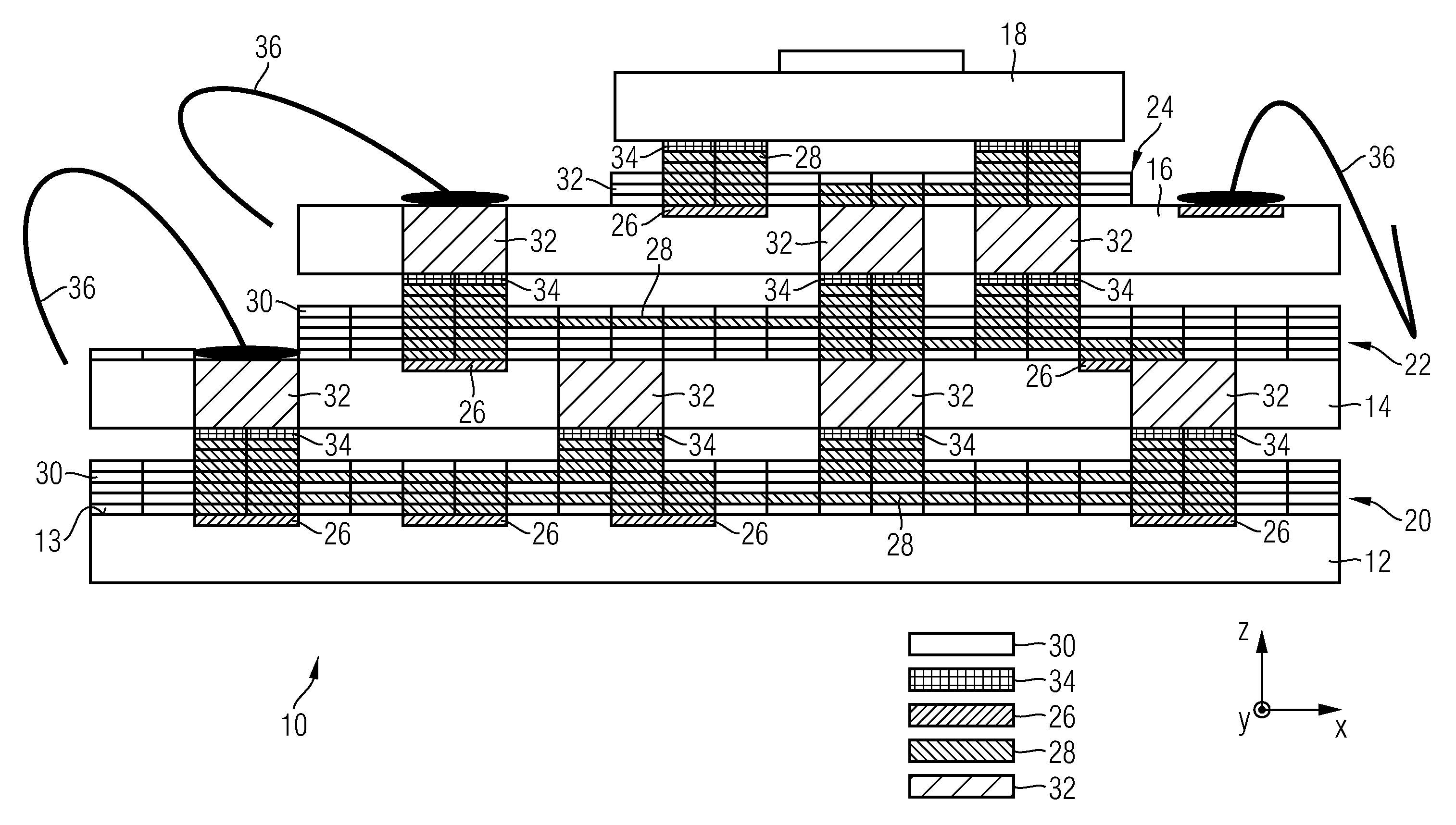
[0050]In the exemplary embodiments described below elements which are similar to one another functionally or structurally are provided as far as possible with the same or similar reference numbers. Therefore, in order to understand the features of the individual elements of a specific exemplary embodiment, reference is made to the description of other exemplary embodiments or to the general description of the invention.

[0051]In order to facilitate the description of the projection exposure tool a Cartesian xyz coordinate system is specified in the drawings from which the respective relative position of the components shown in the figures is clear. In FIG. 1 the y direction runs perpendicular to the plane of the drawing and away from the latter, the x direction to the right, and the z direction upwards.

[0052]FIG. 1 shows a diagrammatic illustration of a semi-conductor module 10 according to the invention in a sectional view. This is a three-dimensionally integrated module in which a ...


PUM


Abstract

In a method for producing a semi-conductor module (10) comprising at least two semi-conductor chips (12, 14) and an interposer (20) which has electrically conductive structures (28) connecting the semi-conductor chips (12, 14) to one another, the interposer (20) is printed directly onto a first (12) of the semi-conductor chips. When the interposer (20) is printed on, the electrically conductive structures (28) are produced by means of electrically conductive ink (68). The second semi-conductor chip (14) is mounted on the interposer (20) such that the two semi-conductor chips (12, 14) are arranged one above the other and that the interposer (20) forms an intermediate layer between the two semi-conductor chips (12, 14).

Description

CROSS-REFERENCE TO RELATED APPLICATIONS[0001]This application is the U.S. National Stage of International Application No. PCT / EP2011 / 000828, filed Feb. 22, 2011, which claims the benefit of German Patent Applications DE 10 2010 008 789.0, filed Feb. 22, 2010, and DE 10 2010 045 372.2, filed Sep. 14, 2010, all of which are hereby incorporated by reference to the extent not inconsistent with the disclosure herewith.BACKGROUND TO THE INVENTION[0002]The invention relates to a semi-conductor module and to a method and a system for producing this type of semi-conductor module.[0003]As mobile electronics become more and more significant, conventional printed circuit boards with active or passive components, such as semi-conductor chips, applied to them two-dimensionally are becoming less significant. The electric or electronic components are stacked three-dimensionally. The aim here is to stack as many chips as possible in the form of a “stack” within the height of an individual housing. T...

Claims


Application Information

Patent Timeline
Patent Type & Authority Patents(United States)
IPC IPC(8): H01L21/00H01L25/065H01L25/00H01L21/48H01L23/538
CPCH01L25/0657H01L25/50H01L21/4867H01L23/538H01L2224/48463H01L2225/0651H01L2225/06513H01L2225/06527H01L2225/06568H01L2225/06572H01L2924/1461H01L2924/00H01L2924/14H01L24/11H01L24/14H01L24/81H01L2224/11318H01L2924/01029H01L2924/01047H01L2924/01079
Inventor JAKOB, ANDREASKAISER, THOMAS
Owner SWISS TECH ENTERPRISE GMBH
Why Eureka
Try Eureka