

Semiconductor structure having common gate and fabrication method thereof
a technology of semiconductors and semiconductors, applied in the direction of semiconductor devices, electrical devices, transistors, etc., can solve the problem of high electrical resistance of common gate formed using conventional gate last technology, and achieve the effect of reducing the resistance of common ga
- Summary
- Abstract
- Description
- Claims
- Application Information
AI Technical Summary
Benefits of technology
Problems solved by technology
Method used
Image

Examples
Embodiment Construction
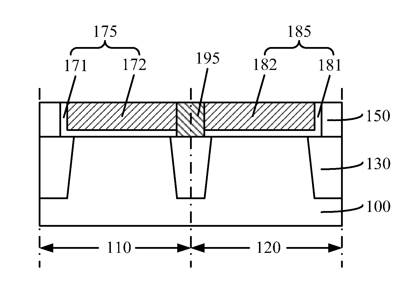
[0015]Reference will now be made in detail to exemplary embodiments of the disclosure, which are illustrated in the accompanying drawings. Wherever possible, the same reference numbers will be used throughout the drawings to refer to the same or like parts.
[0016]Electrical resistance of a common gate formed using gate last technology can be undesirably high. The work functions of the metal gate of NMOS transistor and the metal gate of PMOS transistor are different. Therefore, the metal gate of NMOS transistor and the metal gate of PMOS transistor are formed with different materials and processes, and need to be separately formed.
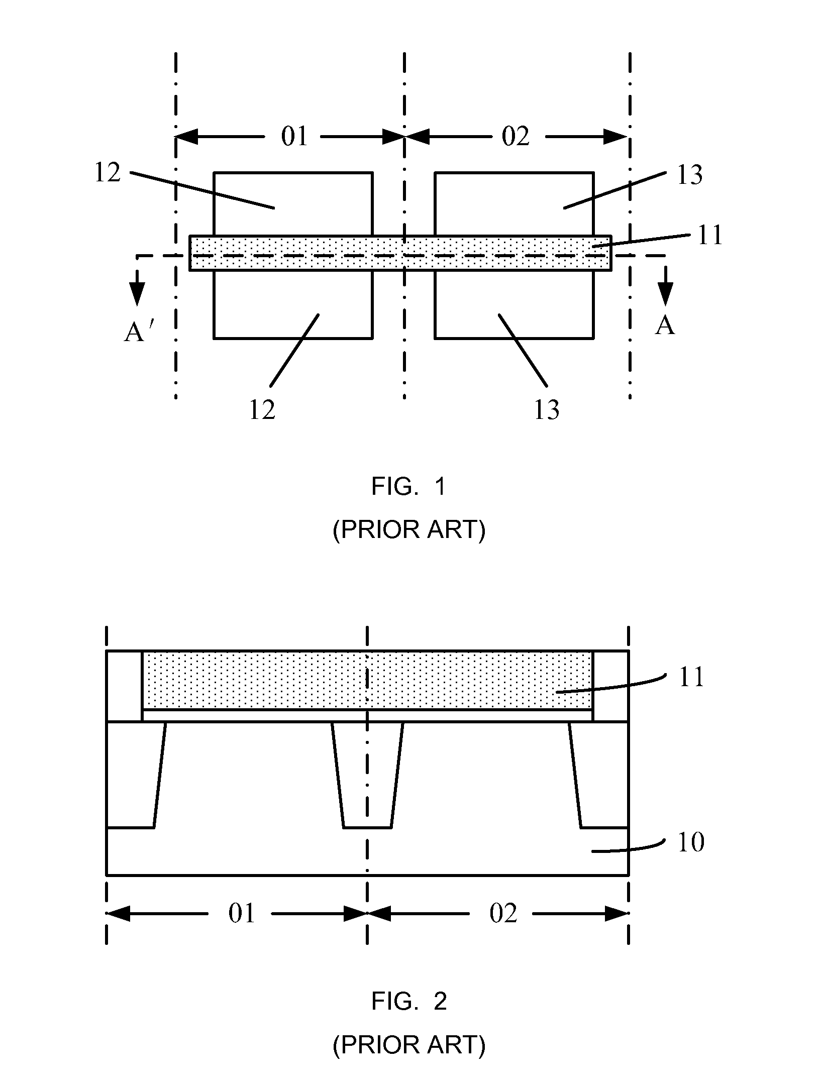
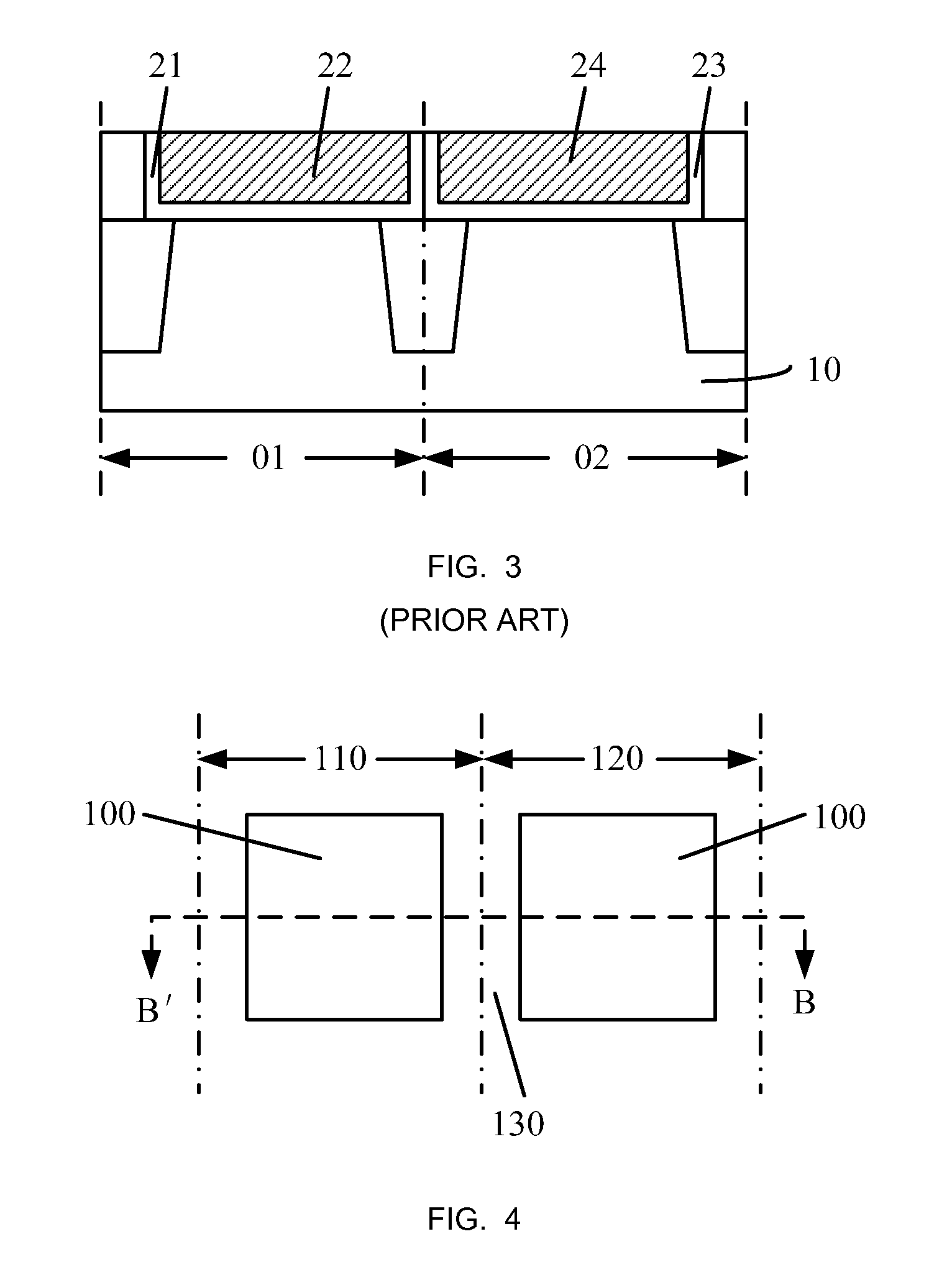
[0017]For example, referring to FIG. 3, a metal gate process for forming the common gate includes: removing a portion of the common gate 11 (e.g., as shown in FIG. 2) in the NMOS transistor region 01 using dry etching process, and forming a first metal gate for the NMOS transistor within a first trench formed by etching. The first metal gate includes a first...
PUM
| Property | Measurement | Unit |
|---|---|---|
| width | aaaaa | aaaaa |
| semiconductor | aaaaa | aaaaa |
| conductive | aaaaa | aaaaa |
Abstract
Description
Claims
Application Information