Method of forming a wiring having carbon nanotube

a carbon nanotube and wiring technology, applied in nanostructure manufacturing, conductive pattern formation, printed circuit manufacturing, etc., can solve the problems of increasing the likelihood of cutting in the metal wiring, affecting the conductive pattern formation process, etc., to achieve the effect of reducing the electrical contact resistance between the carbon nanotube wiring and the upper wiring, reducing the electrical resistance of the wiring, and increasing the adhesiveness between the carbon nanotube wiring and the contact metal layer

Active Publication Date: 2011-02-01
SAMSUNG ELECTRONICS CO LTD
View PDF8 Cites 1 Cited by
  • Summary
  • Abstract
  • Description
  • Claims
  • Application Information

AI Technical Summary

Benefits of technology

[0007]Example embodiments provide a method of forming a wiring including a carbon nanotube to reduce a contact resistance at an interface between a carbon nanotube wiring and a metal wiring.
[0012]According to some example embodiments, there is provided a method of forming a wiring including a carbon nanotube in a semiconductor device. In the method, a lower wiring is formed on a substrate, and a catalyst layer is formed of the lower wiring. An insulating interlayer having an opening which exposes the catalyst layer is formed on the catalyst layer and the substrate. A carbon nanotube is grown from the catalyst layer toward an entrance of the opening. A capping layer is formed on the insulating interlayer to fill the opening in which the carbon nanotube is formed. The capping layer and the carbon nanotube may be partially removed to form a carbon nanotube wiring by performing a CMP process until upper faces of the insulating interlayer and the carbon nanotube are exposed. A native oxide layer is formed on the carbon nanotube wiring while performing the CMP process. The native oxide layer is removed from an upper surface of the carbon nanotube wiring, and the insulating interlayer is partially removed such that an upper portion of the carbon nanotube wiring is protruded from the insulating interlayer. An upper wiring electrically connected to the carbon nanotube wiring is formed on the carbon nanotube wiring and the insulating interlayer. Electrical resistance between the carbon nanotube wiring and the upper wiring in semiconductor device is reduced.
[0015]Accordingly, electrical contact resistance between the carbon nanotube wiring and the upper wiring may be reduced. A portion of a contact metal layer contacting to the carbon nanotube wiring may be partially melted by the thermal stress. Therefore, the carbon nanotube wiring may be electrically or directly connected to the upper wiring via the contact metal layer and electrical resistance of the wiring may further decreases. In addition, adhesiveness between the carbon nanotube wiring and the contact metal layer may also increase, and stability of a device or a manufacturing efficiency may be enhanced.

Problems solved by technology

However, reducing the design rule of the wiring may cause some technical problems.
Hillocks caused by electro-migration (which may increase the likelihood of cuts in the metal wiring) may occur.
Formation of a diffusion barrier layer may become difficult in some applications.
There are some obstacles to the use of a carbon nanotube as a wiring of a semiconductor device.
For example, the carbon nanotube may have poor adhesiveness to a metal and / or high contact resistance at an interface with a metal.
However, when contact resistance between the carbon nanotube and a metal is high, benefits and drawbacks of using the carbon nanotube may offset each other due to an overall increase in resistance.

Method used


Image

  • Method of forming a wiring having carbon nanotube
  • Method of forming a wiring having carbon nanotube
  • Method of forming a wiring having carbon nanotube

Examples


embodiment 1

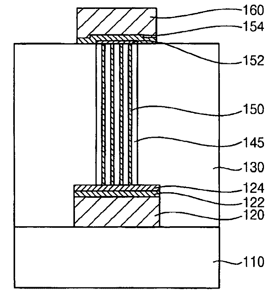
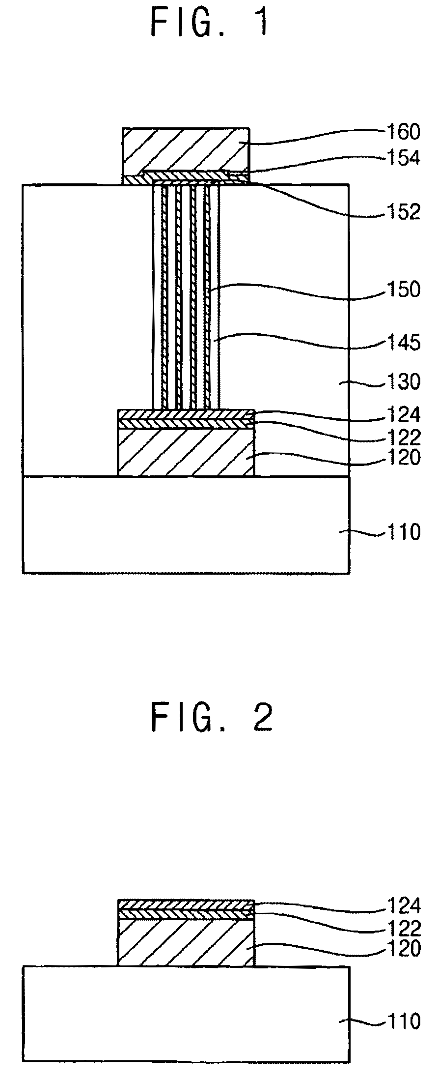
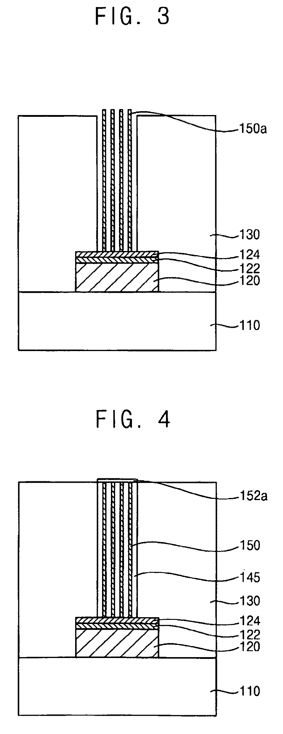
[0037]FIG. 1 is a cross-sectional view illustrating a wiring including a carbon nanotube wiring according to some example embodiments.

[0038]Referring to FIG. 1, a semiconductor device may include a substrate 110, a lower wiring 120 provided on the substrate 110, a first contact metal layer 122, a catalyst layer 124, an insulating interlayer pattern 130, a capping layer pattern 145, a carbon nanotube wiring 150, a native oxide layer 152 being dielectrically broken down, a second contact metal layer 154 and a upper wiring 160.

[0039]The substrate 110 may include a silicon substrate, a silicon germanium substrate, an epitaxial substrate, etc. Several conductive structures may be formed on the substrate 110. Examples of the conductive structures may include a transistor (not illustrated), a capacitor (not illustrated), a contact pad (not illustrated) of the capacitor, which is electrically connected to a first contact region of the transistor, a bit line (not illustrated) electrically co...

embodiment 2

[0067]FIG. 7 is a cross-sectional view illustrating a wiring including a carbon nanotube wiring according to other example embodiments.

[0068]Referring to FIG. 7, a semiconductor device may include a substrate 210, a lower wiring 220 provided on the substrate 210, a first contact metal layer 222, a catalyst layer 224, an insulating interlayer pattern 230, a capping layer pattern 245, a carbon nanotube wiring 250, a second contact metal layer 254 and a upper wiring 260. Description of the first contact metal layer 222, the catalyst layer 224, the insulating interlayer pattern 230, the carbon nanotube wiring 250 and the upper wiring 260 may be the same as that of corresponding elements in Embodiment 1, so description of these elements will not be repeated.

[0069]The capping layer pattern 245 may be formed on the catalyst layer 224 to fill the opening in which the carbon nanotube wiring 250 may be formed. An upper face of the capping layer pattern 245 may be disposed lower than an upper ...

embodiment 3

[0083]FIG. 10 is a cross-sectional view illustrating a decoupling capacitor in a logic device according to another example embodiment.

[0084]Referring to FIG. 10, a decoupling capacitor may include a substrate 300, a ground line 305, a first contact pad 310, a first insulating interlayer 320, a first contact plug 330, a second contact pad 340, a second insulating interlayer 350, a second contact plug 360, a lower electrode 370, a dielectric layer 380, an upper electrode 390 and a protective layer 395.

[0085]The ground line 305 may be provided on the substrate 300. The ground line may be a wiring including carbon nanotube, conductive polysilicon or a metal. The first contact pad 310 may be provided on the substrate. The first contact pad 310 is a first metal wiring and is connected to the ground line 305 or a power line (not illustrated). The first contact pad may include a catalyst layer (not illustrated) and a contact metal layer (not illustrated). The first insulating interlayer 320...


PUM

PropertyMeasurementUnit
currentaaaaaaaaaa
temperatureaaaaaaaaaa
pressureaaaaaaaaaa

Abstract

In a method of forming a wiring having a carbon nanotube, a lower wiring is formed on a substrate, and a catalyst layer is formed on the lower wiring. An insulating interlayer is formed on the substrate to cover the catalyst layer, and an opening is formed through the insulating interlayer to expose an upper face of the catalyst layer. A carbon nanotube wiring is formed in the opening, and an upper wiring is formed on the carbon nanotube wiring and the insulating interlayer to be electrically connected to the carbon nanotube wiring. A thermal stress is generated between the carbon nanotube wiring and the upper wiring to produce a dielectric breakdown of a native oxide layer formed on a surface of the carbon nanotube wiring. A wiring having a reduced electrical resistance between the carbon nanotube wiring and the upper wiring may be obtained.

Description

BACKGROUND[0001]1. Field[0002]Example embodiments relate to a method of forming a wiring including a carbon nanotube. More particularly, example embodiments relate to a method of forming a wiring including a carbon nanotube having reduced contact resistance.[0003]2. Description of the Related Art[0004]Semiconductor devices having high data transmission speed are desired for many applications. One way of increasing the data transmission speed of a semiconductor device may be to increase integration degree in device chips such that a chip includes a large number of cells. A design rule for wirings in semiconductor chips has been reduced to a nanometer scale to increase the integration degree of the cells. However, reducing the design rule of the wiring may cause some technical problems. For example, specific resistance of a wiring may exponentially increase depending on a decrease of a critical dimension of the wiring. Hillocks caused by electro-migration (which may increase the likel...

Claims


Application Information

Patent Timeline
Patent Type & Authority Patents(United States)
IPC IPC(8): H01R43/00H01L21/44
CPCH01L21/76849H01L21/76879H01L23/53276H01L23/5252H01L2221/1094Y10T29/49117H01L2924/0002Y10T29/4913Y10T29/49155H01L2924/00H01L21/28B82Y40/00B82B1/00
Inventor LEE, SUN-WOOMOON, SEONG-HOKIM, DONG-WOOKIM, JUNG-HYEONYOON, HONG-SIK
Owner SAMSUNG ELECTRONICS CO LTD
Why Eureka
Try Eureka