Magnetoresistive random access memory cell and 3D memory cell array

a random access memory and array technology, applied in the field of magnetic random access memory cells and 3d memory cell arrays, can solve problems such as inferior thermal stability, achieve the effects of improving thermal stability, reducing the demagnetization field of thin perpendicular storage layers, and being convenient to implemen

Active Publication Date: 2015-12-22
GE YI +1
View PDF3 Cites 96 Cited by
  • Summary
  • Abstract
  • Description
  • Claims
  • Application Information

AI Technical Summary

Benefits of technology

[0015]In the case of the perpendicular-TMR based SOT-MRAM cell, the above mentioned footprint within the complementary hard magnetic layer, which has perpendicular magnetic easy axis, has the same magnetic orientation as the storage layer. The complementary hard magnetic layer can thermal-stably maintain the magnetic footprint of the data storage layer when the storage layer is set at one direction. It is easy to understand by assuming the complementary hard magnetic layer adjacent to the storage layer is a perpendicular magnetic recording medium locating close to the storage layer, which acts as a perpendicular magnetic writer. The flipping of the storage layer by the SOT effects leads to the change of footprint (or recorded magnetic pattern change). As such, it is easy to know that the knowledge obtained during the development of perpendicular magnetic medium, can be easily implemented here for material design of the complementary hard magnetic layer such as engineering its coercivity and its magnetocrystalline anisotropy. Since the magnetic orientation within the complementary hard magnetic layer has the same orientation as the magnetization of the storage layer, the demagnetization field of thin perpendicular storage layer is dramatically reduced. The magnetic coupling between the complementary hard magnetic and the thin storage layer leads to great improvement of the thermal stability, which effectively means the increase the thickness of the storage layer therefore thermal barrier KV (K is magnetic anisotropy of storage layer, V=S*t is the volume of storage layer) against thermal activation kBT (kB is the Boltzmann, T is the temperature in absolute temperature unit). By adding an optional soft magnetic layer on the other side of the complementary hard magnetic layer, the storage layer will form its own mirrored image within the soft magnetic layer (acting equivalently as so-called soft magnetic underlay in perpendicular magnetic medium). This not only helps the writing the magnetic footprint within the complementary hard magnetic layer but also stabilize the storage layer by further reduce the demagnetization field of the storage layer. As such, our design resolves the problem of inferior thermal stability associate with thin perpendicular storage layer. Since the SOT-MRAM is a three-terminator device with separate writer and read paths, increasing the thickness of the TMR barrier (i.e. MgO thickness) can drastically enhance the TMR ratio for the stack with a thin magnetic storage layer on one side of the TMR barrier. Our design gives a practical design for the perpendicular-TMR stack based SOT-MRAM cell design.
[0016]For in-plane TMR stack based SOT-MRAM cell, as mentioned previously, the biggest challenges of such a design is the magnetic interaction between the storage layers of the adjacent cells. Our design has huge benefit to form a closed magnetic flux loop within each individual cell. The magnetic foot print within complement hard magnetic layer, which has an in-plane magnetic easy axis, has its magnetization direction opposite to the magnetization orientation within the storage layer. The complementary hard magnetic layer can thermal-stably maintain the magnetic footprint of the data storage layer when the storage layer is set at one direction. It is easy to understand by assuming the complementary hard magnetic layer adjacent to the storage layer is a longitudinal magnetic recording medium locating close to the storage layer, which acts as a longitudinal magnetic writer. As such, it is easy to know that the knowledge obtained during the development of longitudinal magnetic medium, can be easily implemented here for material design of complementary hard magnetic layer such as engineering its coercivity. The flipping of the storage layer by the SOT effects leads to the footprint change (or recorded magnetic pattern change). Since the flux emitting from the storage layer and the one from its ‘opposite’ magnetic footprint within the complementary magnetic hard layer forms a closed magnetic flux loop. It helps to not only further stabilize the storage layer but also cancel the free flux emitted from the storage layer. By material engineering refinement, the totally flux can fully cancel each other, which leads zero total fringe magnetic field emitted out from the individual SOT-MRAM cell. Just as the perpendicular case, an optional soft magnetic layer can be placed on the other side of the complementary magnetic layer. But it is definitely is not a must as it could bring more magnetic complications.
[0017]Apart from SOT-MARM cells designs for both perpendicular and in-plane TMR stack based system, we also proposed a novel electrical connection and memory array architectural design and cell sensing scheme. Our proposal of using constant sensing voltage on read line and measuring the cell voltage on level line whiling sharing only one access transistor for all memory cells stacked on one 2D cell footprint (detailed description will be given in following sections) facilitates much simpler 3D integration capability for our SOT-MRAM array design. The design not only can extend in 2D, but also can expand to the third dimension, which greatly enhances the area density of the SOT-MRAM design.

Problems solved by technology

As such, our design resolves the problem of inferior thermal stability associate with thin perpendicular storage layer.
For in-plane TMR stack based SOT-MRAM cell, as mentioned previously, the biggest challenges of such a design is the magnetic interaction between the storage layers of the adjacent cells.
But it is definitely is not a must as it could bring more magnetic complications.

Method used


Image

  • Magnetoresistive random access memory cell and 3D memory cell array
  • Magnetoresistive random access memory cell and 3D memory cell array
  • Magnetoresistive random access memory cell and 3D memory cell array

Examples


Embodiment Construction

[0034]The following description is provided in the context of particular designs, applications and the details, to enable any person skilled in the art to make and use the invention. However, for those skilled in the art, it is apparent that various modifications to the embodiments shown can be practiced with the generic principles defined here, and without departing the spirit and scope of this invention. Thus, the present invention is not intended to be limited to the embodiments shown, but is to be accorded the widest scope consistent with the principles, features and teachings disclosed here.

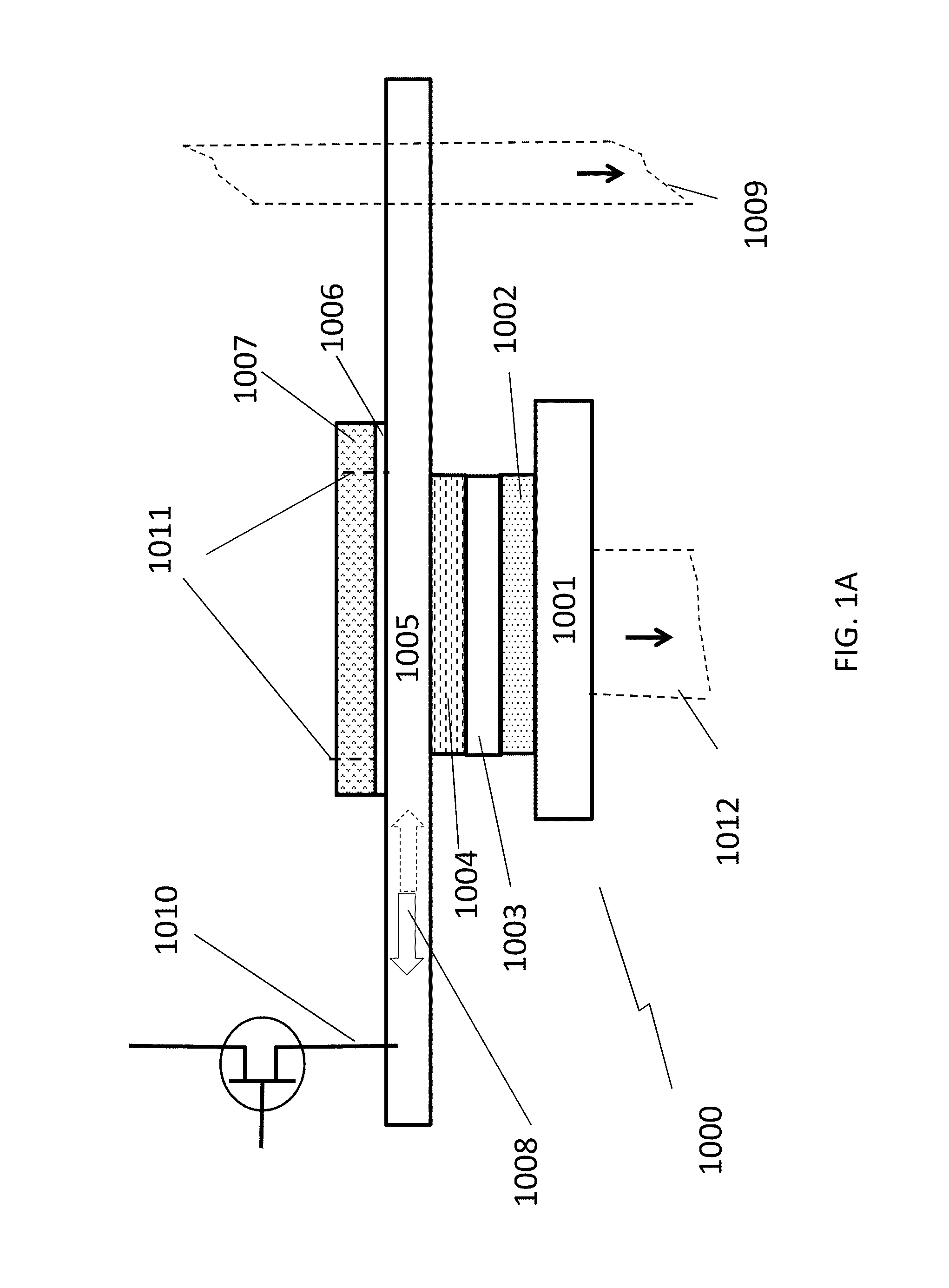
[0035]FIG. 1A illustrates one embodiment of the cross section drawings for general description of the proposed SOT-MRAM cell structure 1000. The purpose of FIG. 1A is to demonstrate the most important invention of the proposed SOT-MRAM cell design. In the proposed SOT-MRAM cell 1000 as shown in FIG. 1A, a TMR stack, including a reference layer 1002, a tunneling barrier 1003 (e.g. MgO), and a...


PUM


Abstract

A novel three-terminal SOT-MRAM memory cell with a unique magnetic stabilization layer or structure is proposed. A complementary magnetic footprint of the data storage layer for the memory cell is able to be created within the magnetic stabilization layer or structure by the magnetic field from the storage layer to enhance the magnetic and thermal stability of the memory cell. Several designs for both perpendicular and in-plane SOT-MRAM memory cell have been invented. With proper wire connection and sensing arrangement, the proposed memory cell is capable of forming not only the 2D array but also 3D array.

Description

RELATED APPLICATIONS[0001]The present application claims of the priority benefit of U.S. patent application Ser. No. 13 / 288,860 filed on Nov. 3, 2011 as Utility application, published on May 9, 2013 as US2013 / 0114334A1 entitled “MAGNETORESISTIVE RANDOM ACCESS MEMORY CELL WITH INDEPENDENTLY OPERATING READ AND WRITE COMPONENTS”, which is incorporated herein by reference.FIELD OF INVENTION[0002]The invention is related to magnetoresistive random access memory cell design and how to stack multiple cells on one 2D footprint to form a 3D memory cell array to increase area density of the memory. Particularly, the so-called spin-orbit torque magnetoresistive random access memory (SOT-MRAM) cell design and 3D integration to resolve some long standing issues related to this new class of MRAM.BACKGROUND ART[0003]Data storage memory is one of the backbones of the modern information technology. Semiconductor memory in the form of Dynamic random-access memory (DRAM), Static random-access memory (...

Claims


Application Information

Patent Timeline
Patent Type & Authority Patents(United States)
IPC IPC(8): G11C11/00G11C11/16
CPCG11C11/161G11C11/1675G11C11/1673G11C11/18G11C2213/71G11C11/1653G11C11/1659H10B61/22H10N50/10
Inventor YI, GELI, DONG
Owner GE YI
Why Eureka
Try Eureka