Layers for increasing performance in image sensors

a technology of image sensor and layer, applied in the field of backside illumination of image sensor, can solve problems such as degrading the sensitivity of image sensor

Active Publication Date: 2015-12-29
OMNIVISION TECH INC
View PDF15 Cites 2 Cited by
  • Summary
  • Abstract
  • Description
  • Claims
  • Application Information

AI Technical Summary

Benefits of technology

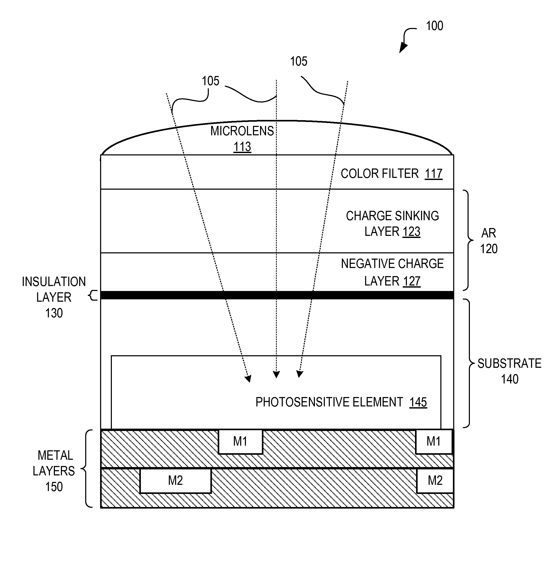
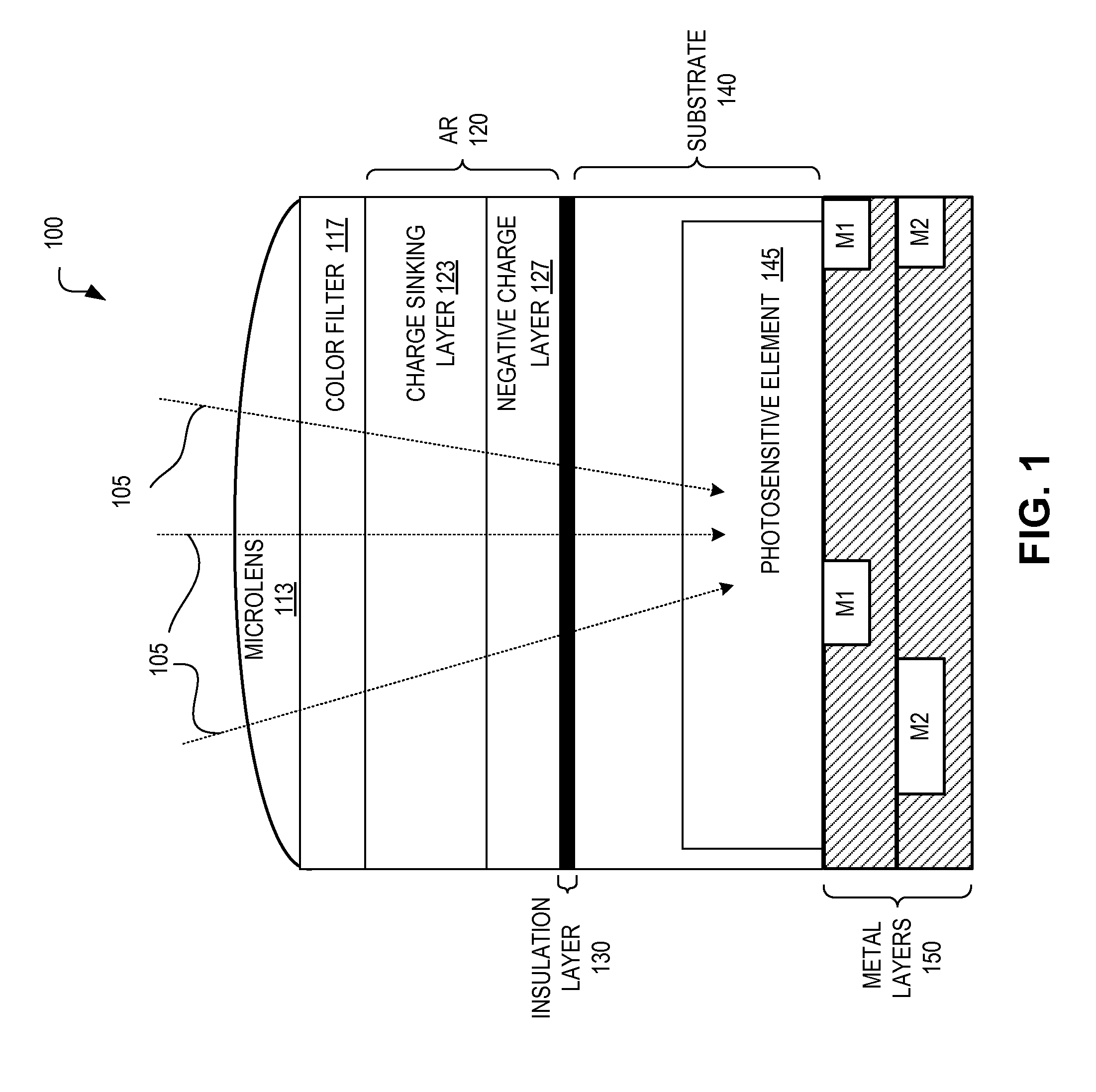
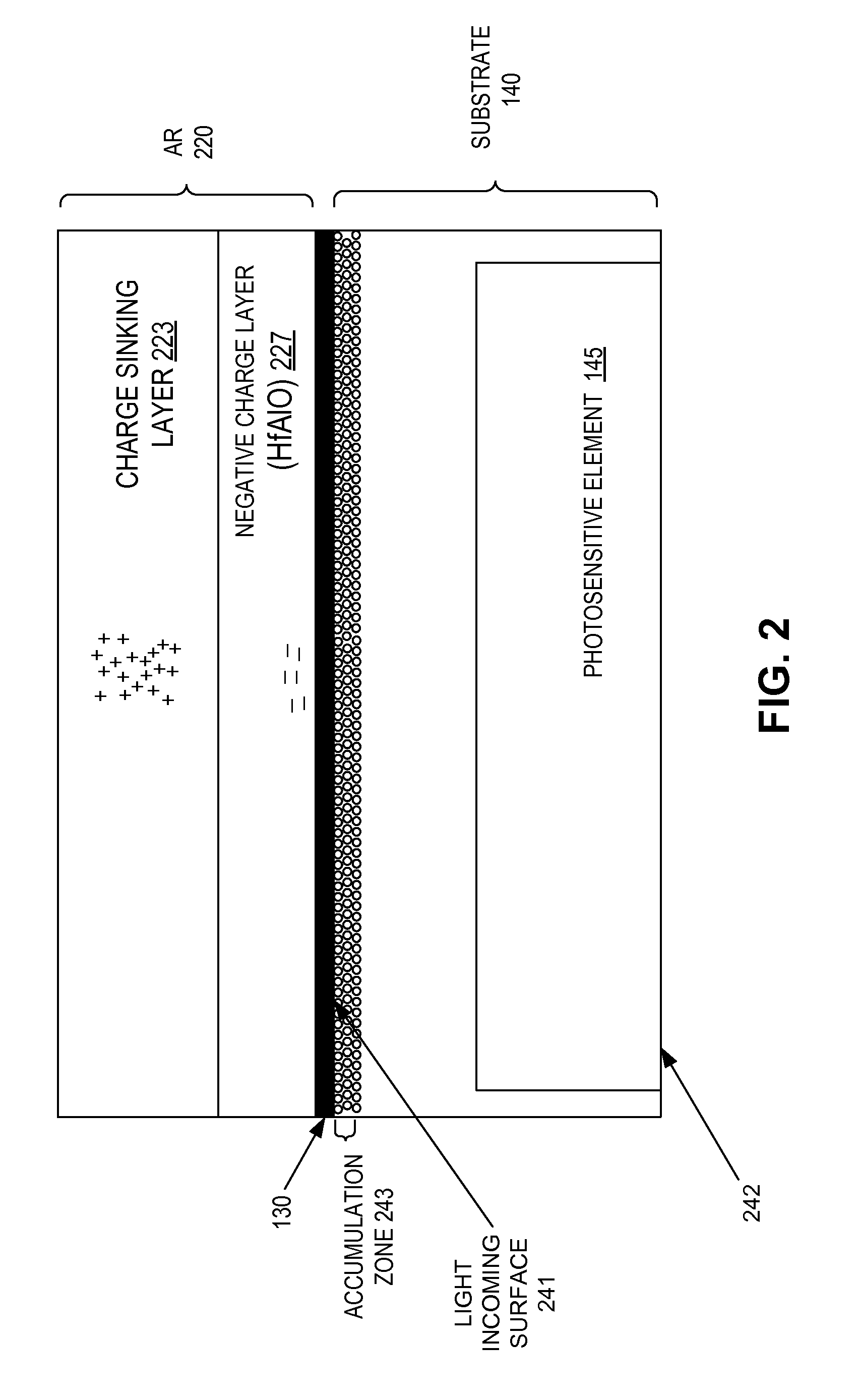
[0003]Backside illuminated (“BSI”) technology is often used in image sensors to increase the amount of image light that becomes incident on photosensitive elements in pixels of the image sensor. When BSI technology is used, backside accumulation helps create an electric field that directs photo-electrons (generated by incident image light) to a frontside of the image sensor where they can be collected and measured. Without accumulation on the backside the semiconductor substrate, diffusion of the electrons to the back surface may result in loss by recombination, which may degrade the sensitivity of the image sensor. Advantageously, accumulation on the backside of the semiconductor substrate can reduce or impede “dark current” generated from the semiconductor substrate's interface with another layer (e.g. silicon dioxide insulation layer). Reducing “dark current” will improve the signal-to-noise ratio of the image sensor, which importantly, improves the sensitivity of the image sensor. Given that accumulation on the backside of the semiconductor substrate is beneficial, the image sensor industry seeks to generate backside accumulation that will give image sensors improved performance.

Problems solved by technology

Without accumulation on the backside the semiconductor substrate, diffusion of the electrons to the back surface may result in loss by recombination, which may degrade the sensitivity of the image sensor.

Method used


Image

  • Layers for increasing performance in image sensors
  • Layers for increasing performance in image sensors
  • Layers for increasing performance in image sensors

Examples


Embodiment Construction

[0018]Embodiments of an image sensor and an imaging system are described herein. In the following description, numerous specific details are set forth to provide a thorough understanding of the embodiments. One skilled in the relevant art will recognize, however, that the techniques described herein can be practiced without one or more of the specific details, or with other methods, components, materials, etc. In other instances, well-known structures, materials, or operations are not shown or described in detail to avoid obscuring certain aspects.

[0019]Reference throughout this specification to “one embodiment” or “an embodiment” means that a particular feature, structure, or characteristic described in connection with the embodiment is included in at least one embodiment of the present invention. Thus, the appearances of the phrases “in one embodiment” or “in an embodiment” in various places throughout this specification are not necessarily all referring to the same embodiment. Fu...


PUM


Abstract

An imaging device includes a semiconductor substrate having a photosensitive element for accumulating charge in response to incident image light. The semiconductor substrate includes a light-receiving surface positioned to receive the image light. The imaging device also includes a negative charge layer and a charge sinking layer. The negative charge layer is disposed proximate to the light-receiving surface of the semiconductor substrate to induce holes in an accumulation zone in the semiconductor substrate along the light-receiving surface. The charge sinking layer is disposed proximate to the negative charge layer and is configured to conserve or increase an amount of negative charge in the negative charge layer. The negative charge layer is disposed between the semiconductor substrate and the charge sinking layer.

Description

TECHNICAL FIELD[0001]This disclosure relates generally to image sensors, and in particular but not exclusively, relates to backside illuminated image sensors.BACKGROUND INFORMATION[0002]Image sensors are widely used in digital still cameras, cellular phones, security cameras, as well as in, medical, automobile, and other applications. Complementary metal-oxide-semiconductor (“CMOS”) technology is used to manufacture lower cost image sensors on silicon substrates. In a large number of image sensors, the image sensor commonly includes hundreds, thousand or even millions of light sensor cells or pixels.[0003]Backside illuminated (“BSI”) technology is often used in image sensors to increase the amount of image light that becomes incident on photosensitive elements in pixels of the image sensor. When BSI technology is used, backside accumulation helps create an electric field that directs photo-electrons (generated by incident image light) to a frontside of the image sensor where they ca...

Claims


Application Information

Patent Timeline
Patent Type & Authority Patents(United States)
IPC IPC(8): H01L21/02H01L31/0216H01L27/146
CPCH01L31/02161H01L27/1464H01L27/1462
Inventor HSIUNG, CHIH-WEICELLEK, ORAY ORKUNCHEN, GANGMAO, DULIVENEZIA, VINCENTTAI, HSIN-CHIH
Owner OMNIVISION TECH INC
Why Eureka
Try Eureka