
Semiconductor device

a technology of semiconductor devices and shielding rings, applied in semiconductor devices, semiconductor/solid-state device details, electrical apparatus, etc., can solve the problems of limiting the improvement of breakdown voltage, and the large area of the guard ring structure to retain breakdown voltage, etc., and achieve the effect of stabilizing the breakdown voltag

Active Publication Date: 2016-01-12
ARIGNA TECH LTD
View PDF18 Cites 0 Cited by
  • Summary
  • Abstract
  • Description
  • Claims
  • Application Information

AI Technical Summary

Benefits of technology

The present invention provides a field plate for a semiconductor device that prevents concentration of electric field just below the guard ring electrode attached to the outermost guard ring, which results in stabilized breakdown voltage. The field plate has two portions that are capacitively coupled to the guard ring electrode and the channel stopper electrode, respectively. This arrangement ensures that the electric field is evenly distributed and prevents any electrical arcing.

Problems solved by technology

Unfortunately, this limits improvement of breakdown voltage just below the guard ring electrode attached to the outermost guard ring.
Also, the guard ring structure unfortunately requires a large area to retain breakdown voltage.

Method used


Image

  • Semiconductor device
  • Semiconductor device
  • Semiconductor device

Examples


first embodiment

[0023]First, a configuration of a semiconductor device of a first embodiment of the present invention will be described.

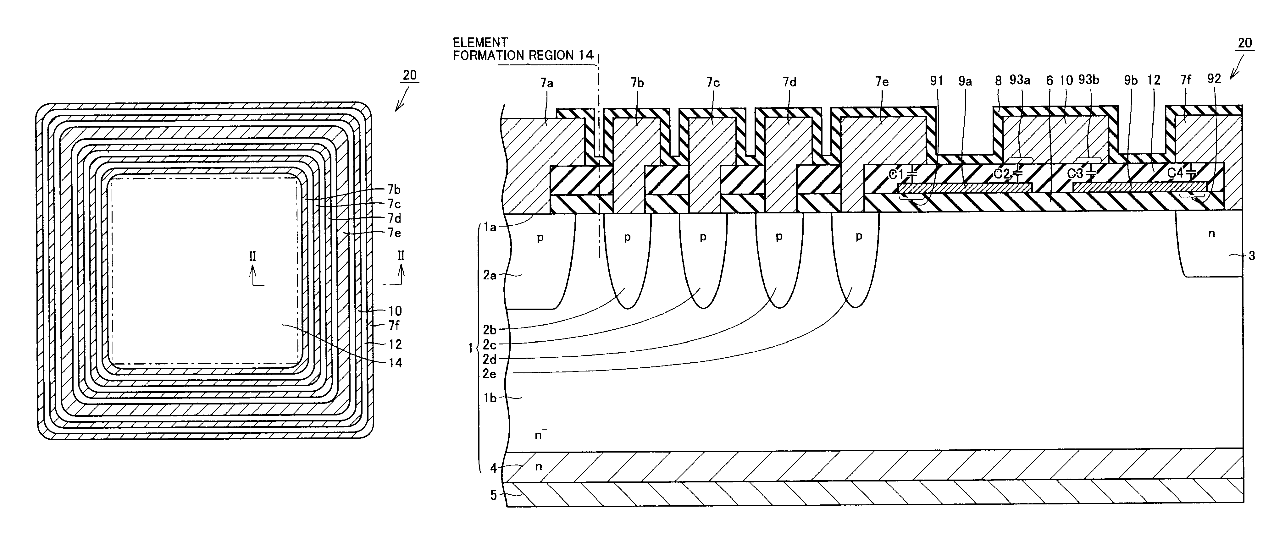
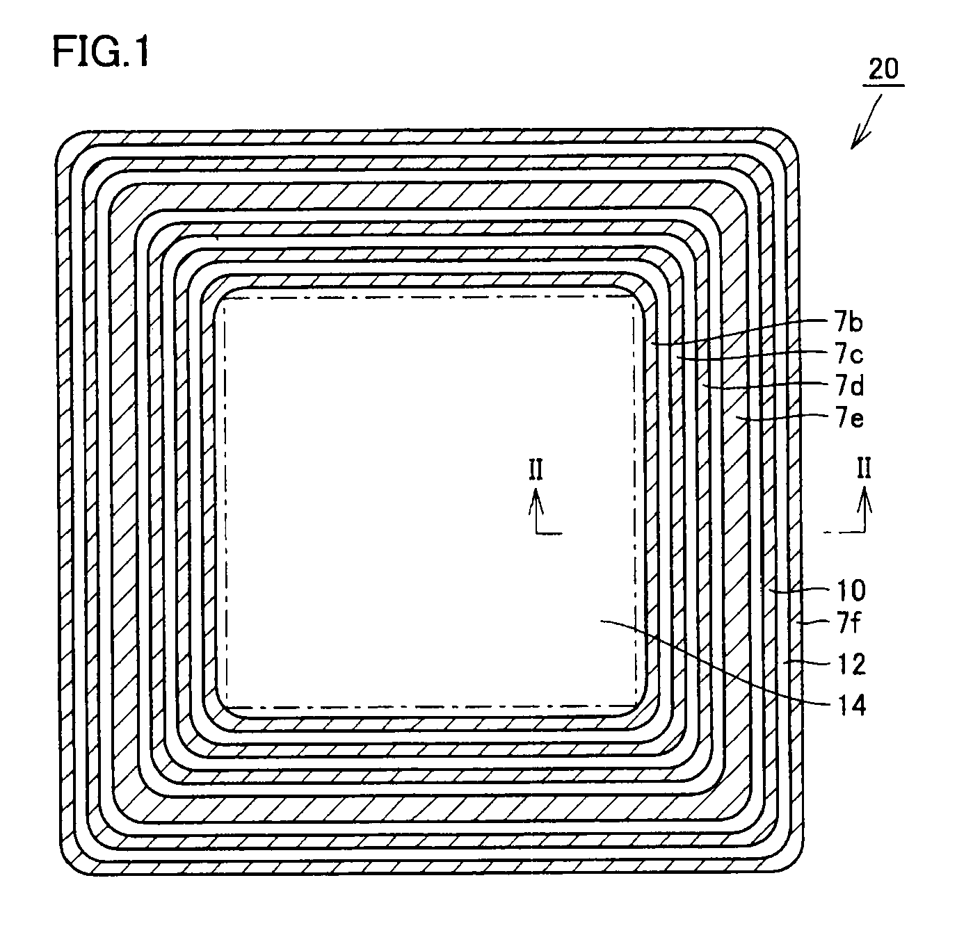
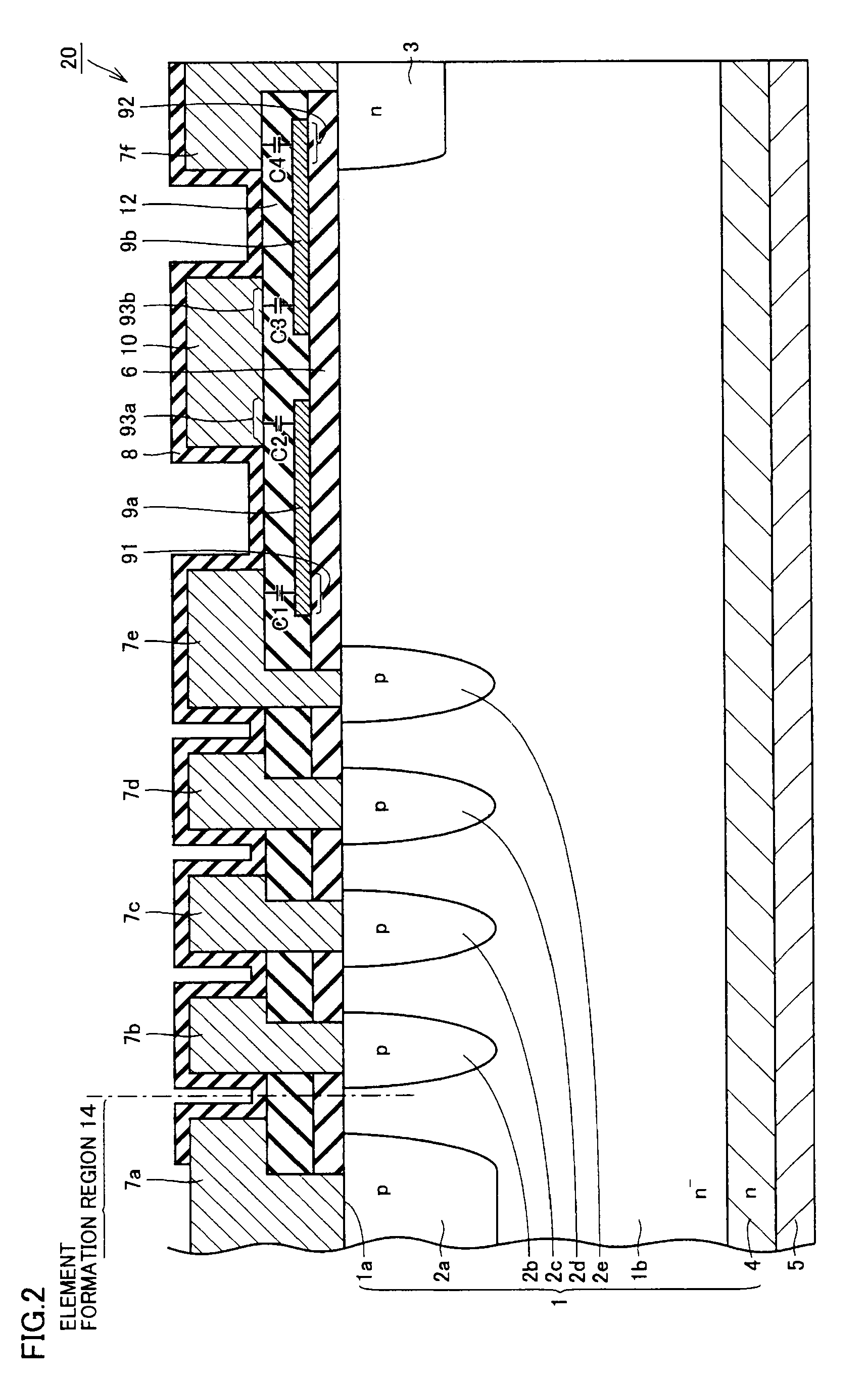
[0024]Referring to FIG. 1 and FIG. 2, semiconductor device 20 of the present embodiment mainly has a semiconductor substrate 1, a collector electrode 5, a field oxide film 6, an emitter electrode 7a, guard ring electrodes 7b, 7c, 7d, 7e, a channel stopper electrode 7f, and field plates 9a, 9b, 10. For visibility, a passivation film 8 is not drawn in FIG. 1.

[0025]Referring to mainly FIG. 1, when viewed in a plan view, semiconductor device 20 has a central portion provided with a formation region 14 for a power semiconductor element such as an IGBT (Insulated Gate Bipolar Transistor). When viewed in the plan view, guard ring electrodes 7b, 7c, 7d, 7e are formed to surround a circumference of element formation region 14. When viewed in the plan view, field plate 10 and channel stopper electrode 7f are formed to surround the circumference of guard ring electrode 7e.

[0...

second embodiment

[0053]A semiconductor device of a second embodiment of the present invention is different from the semiconductor device of the first embodiment mainly in configurations of field plates.

[0054]Referring to FIG. 3 and FIG. 4, semiconductor substrate 1 has a main surface 1a over which field plates 9a, 9b are formed with a field oxide film 6 interposed between main surface 1a and field plates 9a, 9b. For visibility, in FIG. 3, a passivation film 8 is not drawn.

[0055]Formed on field plates 9a, 9b is an insulation film 13 on which a field plate 9c (third portion) is formed. On field plate 9c, an interlayer insulation film 12 is formed. On interlayer insulation film 12, a guard ring electrode 7e and a channel stopper electrode 7f are formed. In other words, field plate 9c (third portion) is formed as a layer below guard ring electrode 7e and channel stopper electrode 7f.

[0056]When viewed in a plan view, field plate 9c (third portion) has a portion 93a overlapping with field plate 9a (first...

third embodiment

[0062]A semiconductor device of a third embodiment of the present invention is different from the semiconductor device of the first embodiment in configurations of field plates.

[0063]Referring to FIG. 5, semiconductor substrate 1 has a main surface 1a over which field plates 9a, 9b are formed with a field oxide film 6 interposed between main surface 1a and field plates 9a, 9b. Field plates 9c (third portion) are formed between field plates 9a, 9b and an interlayer insulation film 12 is provided among them. In the present embodiment, two field plates 9c (third portion) are described but the present invention is not limited to this. A single or a plurality of field plates 9c may be provided. Field plates 9a, 9b, 9c are arranged along a direction in which main surface 1a of semiconductor substrate 1 extends. Field plates 9a, 9b, 9c overlap with their adjacent field plates 9a, 9b, 9c in the direction in which main surface 1a extends.

[0064]In the direction in which main surface 1a extend...


PUM


Abstract

A semiconductor device includes: a semiconductor substrate having a main surface having an element formation region, a guard ring, a guard ring electrode, a channel stopper region, a channel stopper electrode, and a field plate disposed over and insulated from the semiconductor substrate. The field plate includes a first portion located between the main surface of the semiconductor substrate and the guard ring electrode, and a second portion located between the main surface of the semiconductor substrate and the channel stopper electrode. The first portion has a portion overlapping with the guard ring electrode when viewed in a plan view. The second portion has a portion overlapping with the channel stopper electrode when viewed in the plan view. In this way, a semiconductor device allowing for stabilized breakdown voltage can be obtained.

Description

BACKGROUND OF THE INVENTION[0001]1. Field of the Invention[0002]The present invention relates to a semiconductor device, in particular, to a semiconductor device having a guard ring.[0003]2. Description of the Background Art[0004]Generally, a power semiconductor requires a high main breakdown voltage retaining capability. For such retention of breakdown voltage, guard ring structures are generally utilized. Basic structures and applied structures thereof are disclosed in, for example, the following document or the like:[0005]B. Jayant Baliga, “Power Semiconductor Devices”, the United States, PWS PUBLISHING COMPANY, pp. 98-103[0006]A guard ring structure is provided with an impurity region having a floating potential and surrounding an emitter to alleviate surface electric field and retain breakdown voltage.[0007]If guard rings are provided up to the end of a semiconductor substrate, an electric field peak comes in the semiconductor substrate in the vicinity of its central portion in...

Claims


Application Information

Patent Timeline
Patent Type & Authority Patents(United States)
IPC IPC(8): H01L23/58H01L29/40H01L29/06H01L29/739
CPCH01L29/404H01L29/0619H01L29/7395H01L29/0638
Inventor TAKAHASHI, TETSUOOTSUKI, TAKAMI
Owner ARIGNA TECH LTD
Learn More