A normally-off hemt device with a honeycomb groove barrier layer structure under a field plate and its preparation method
A technology of barrier layer and normally-off type, which is applied in the field of normally-off HEMT devices and its preparation, and can solve the problems of increased on-resistance of manufactured devices, difficulty in ensuring uniformity of etching, and damage to barrier layers, etc.
- Summary
- Abstract
- Description
- Claims
- Application Information
AI Technical Summary
Problems solved by technology
Method used
Image
Examples
Embodiment 1
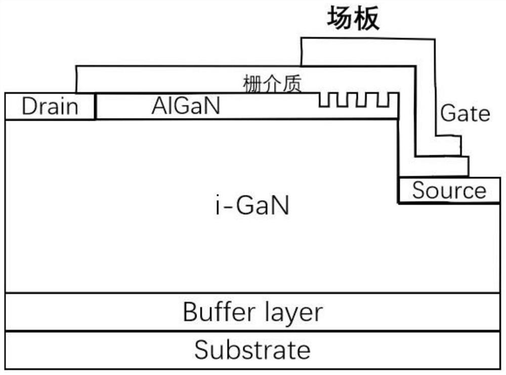
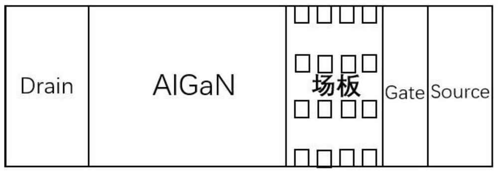
[0034] A normally-off HEMT device with a honeycomb groove barrier layer structure below the field plate, a buffer layer, an i-GaN layer, an insertion layer, a barrier layer and a gate dielectric layer are sequentially grown on a semiconductor substrate, and the barrier layer A number of honeycomb grooves are etched in the local area of the i-GaN layer, one side of the i-GaN layer is etched into a step layer, a source electrode is set on the step layer, and a drain electrode is set on the other side of the i-GaN layer, the A gate dielectric layer is arranged above the barrier layer, one end of the gate dielectric layer is in contact with the drain electrode, the other end covers and grows into the honeycomb groove, and extends to the source electrode, and above the gate dielectric layer . A gate electrode is arranged in a region corresponding to the honeycomb groove, and the gate electrode extends toward the source electrode.
[0035] The substrate is Si, the buffer layer is ...
Embodiment 2
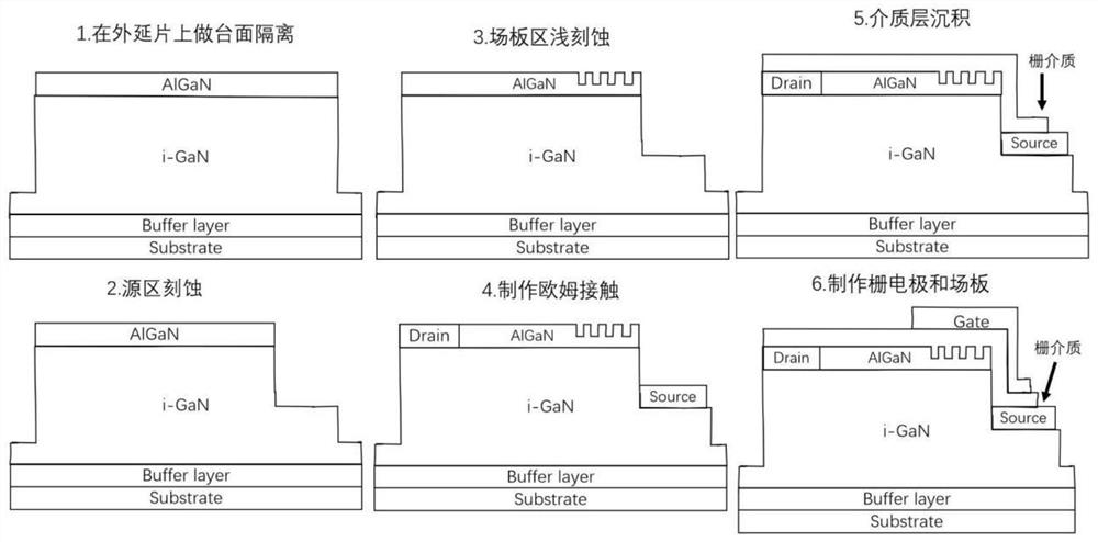
[0047] The production process of the specific embodiment of the target device of this embodiment is described as follows:
[0048] a) Epitaxial growth: an AlGaN / GaN epitaxial layer is epitaxially grown on a Si substrate, and the epitaxial layer includes a GaN buffer layer, an i-GaN layer, an AlN insertion layer, and an AlGaN barrier layer in sequence from bottom to top.
[0049] b) Device isolation: After photolithography and development of the sample, the sample was etched with a depth of 800 nm using an ICP device using Cl-based gas.
[0050] c) Etching of the source region: After the photolithographic development of the sample, the source region is etched with a depth of 500nm using Cl-based gas using ICP equipment. During this process, the etching step is ensured by optimizing the ICP etching power and gas flow The side walls are relatively smooth.
[0051] d) Shallow etching in the field plate area: After the photolithographic development of the sample, ICP equipment is ...
PUM
| Property | Measurement | Unit |
|---|---|---|
| width | aaaaa | aaaaa |
| depth | aaaaa | aaaaa |
| thickness | aaaaa | aaaaa |
Abstract
Description
Claims
Application Information


