Power device having interface charge trench high-voltage interconnection structure
A technology of interface charge and interconnection structure, applied in the direction of electrical components, semiconductor devices, circuits, etc., to achieve the effect of stabilizing the breakdown voltage
- Summary
- Abstract
- Description
- Claims
- Application Information
AI Technical Summary
Problems solved by technology
Method used
Image
Examples
Embodiment 1
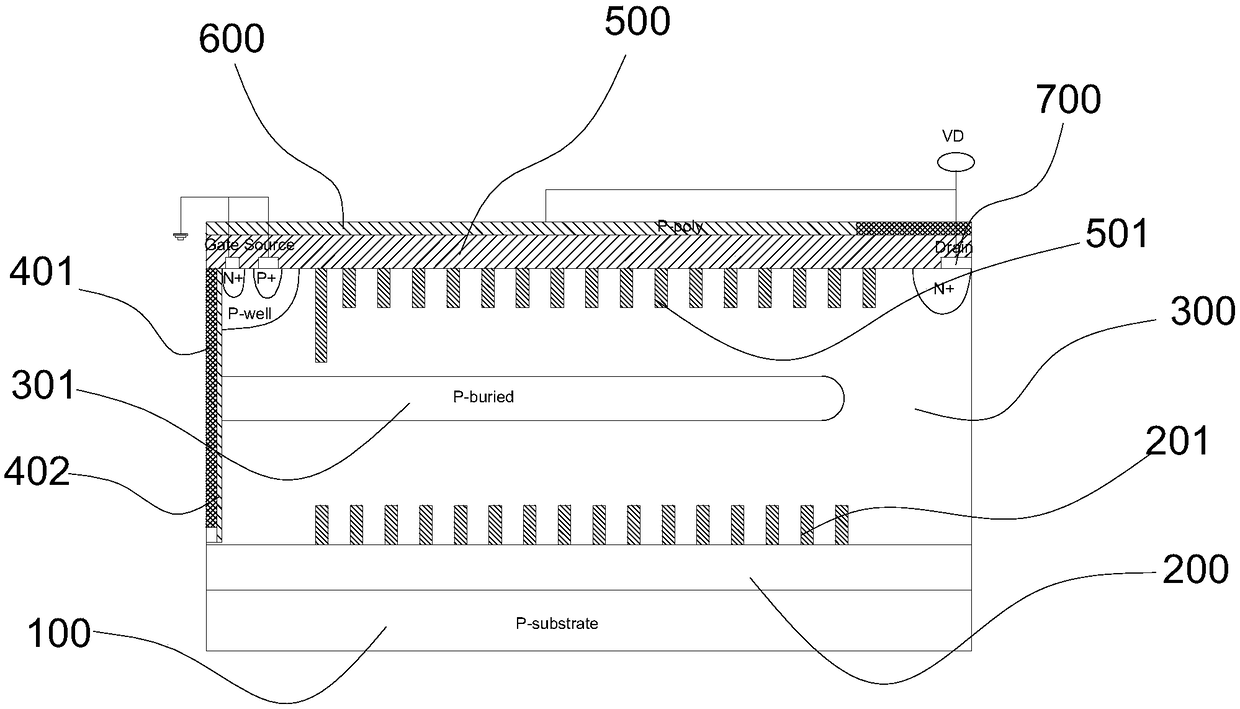
[0037] Such as image 3 The shown power device with an interface charge slot high-voltage interconnection structure includes a drift region 300, a buried layer 200, and a substrate 100 arranged in sequence from top to bottom; the drift region 300 is provided with N + Drain region, drain electrode 700, gate electrode, source electrode, N + Contact area, p-well and P + source region; the outer surface of one side of the drift region 300 is provided with a vertical gate; the vertical gate is a vertical groove gate formed by polysilicon 401 and a vertical oxide layer 402; the groove gate extends to the buried layer 200; The trench gate and the p-well form a vertical conductive channel; the drift region 300 is provided with a horizontal P-type buried layer 301 connected to the vertical gate;
[0038] A buried layer 2 500 is disposed above the drift region 300, and a surface structure 600 is disposed above the buried layer 500; a vertical dielectric trench 201 extending into the d...
PUM
 Abstract
Description
Claims
Application Information


