CVD oxide surface pre-conditioning by inductively coupled O2 plasma

a technology of inductive coupling and o2 plasma, which is applied in the direction of semiconductor/solid-state device manufacturing, basic electric elements, electric apparatus, etc., can solve the problems of native oxide contamination, difficulty in processing, and undesirable native oxides

Active Publication Date: 2016-01-19
APPLIED MATERIALS INC
View PDF5 Cites 115 Cited by
  • Summary
  • Abstract
  • Description
  • Claims
  • Application Information

AI Technical Summary

Problems solved by technology

Native oxides may also result from contamination during etching processes.
Native oxides are typically undesirable and need to be removed prior to a subsequent processing.
Some oxide features may have two or more oxides that respond differently to the same process, hence posing difficulties in processing, especially at advanced technology nodes, such as sub-10 nm nodes.
However, sputter etching processes generally cannot completely remove oxides and can damage delicate silicon

Method used


Image

  • CVD oxide surface pre-conditioning by inductively coupled O2 plasma
  • CVD oxide surface pre-conditioning by inductively coupled O2 plasma
  • CVD oxide surface pre-conditioning by inductively coupled O2 plasma

Examples


Embodiment Construction

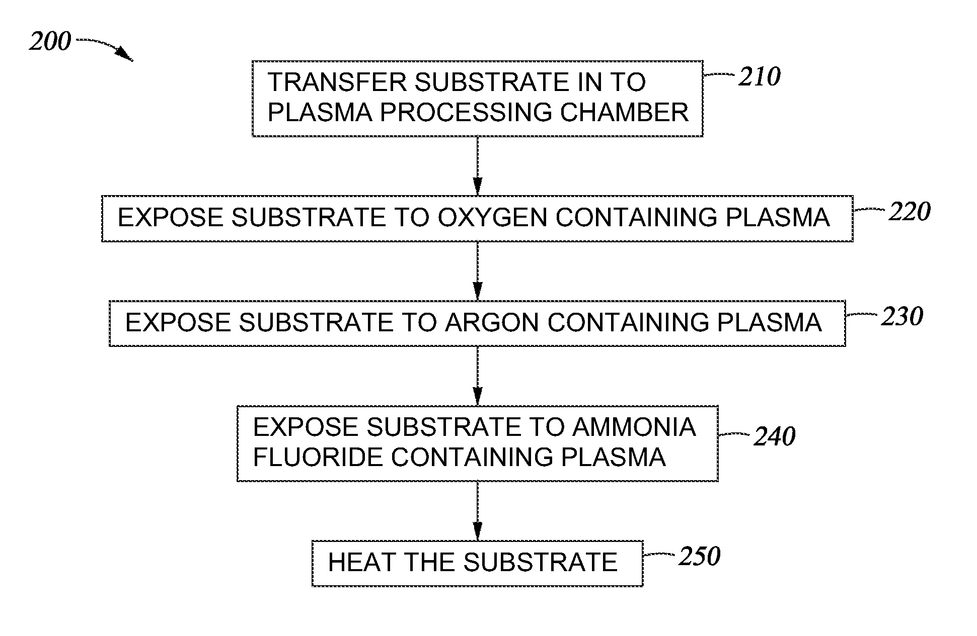
[0022]A method and apparatus for conditioning an oxide surface during a semiconductor device formation process is provided herein. One or more plasma processing operations are performed on a substrate having a fin structure and shallow trench isolation structure (STI) formed thereon. An oxygen containing plasma process may modify surfaces of the STI structure in preparation for an argon containing plasma process. The argon containing plasma process may form a first layer on the fin structure and STI structure and an ammonia fluoride containing plasma process may form a second layer on the first layer. The first and second layers may be removed from the substrate during a subsequent heating process to provide a cleaned fin structure suitable for subsequent processing operations.

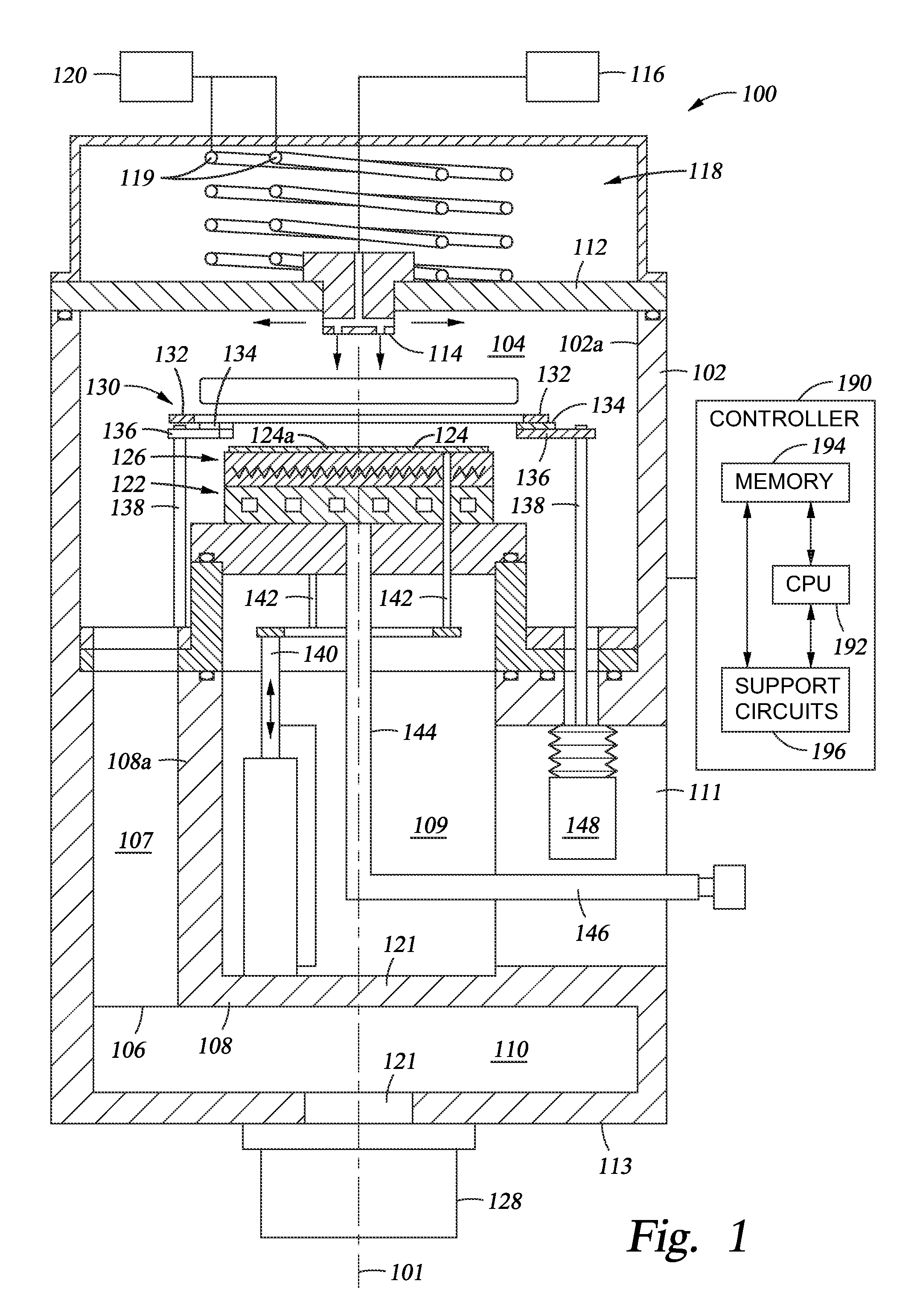
[0023]FIG. 1 illustrates a schematic, cross-sectional view of a plasma processing chamber 100 within which embodiments of the disclosure may be performed. One example of a plasma processing chamber within whic...


PUM


Abstract

A method and apparatus for conditioning an oxide surface during a semiconductor device formation process is provided herein. One or more plasma processing operations are performed on a substrate having a fin structure and shallow trench isolation structure (STI) formed thereon. An oxygen containing plasma process may modify surfaces of the STI structure in preparation for an argon containing plasma process. The argon containing plasma process may form a first layer on the fin structure and STI structure and an ammonia fluoride containing plasma process may form a second layer on the first layer. The first and second layers may be removed from the substrate during a subsequent heating process to provide a cleaned fin structure suitable for subsequent processing operations.

Description

BACKGROUND[0001]1. Field[0002]Embodiments of the present disclosure generally relate to methods and apparatus for forming a semiconductor device. More specifically, embodiments described herein relate to a chemical vapor deposition (CVD) oxide surface preconditioning process.[0003]2. Description of the Related Art[0004]In semiconductor fabrication, oxide fabrication is critical, especially for thin layer oxides which is an essential part of gate structure for Complimentary Metal Oxide Semiconductor (CMOS) technology. With proper manufacturing control, oxide layers exhibit stable and desirable dielectric properties. A variety of oxide fabrication processes are used in integrated device manufacturing (IDM) to obtain oxides of different properties for different functions. Thermal oxides and deposited oxides are most commonly used in semiconductor devices. Additionally, native oxides may be generated during processing. Different oxides may also respond differently to subsequent processe...

Claims


Application Information

Patent Timeline
IPC IPC(8): H01L21/02
CPCH01L21/02164H01L21/02238H01L21/02315H01L21/02334H01L21/02057H01L21/0206H01L21/02299
Inventor HSIEH, PING HANKUO, TENG-FANG
Owner APPLIED MATERIALS INC
Why Eureka
Try Eureka