Method for fastening chips with a contact element onto a substrate provided with a functional layer having openings for the chip contact elements

a contact element and functional layer technology, applied in the direction of solid-state device manufacturing, electric devices, semiconductor/solid-state device manufacturing, etc., can solve the problems of limiting the choice of materials, unable to implement the above sequence, and the electrical contact between the chips and the substrate poses technical problems, etc., to achieve improved electrical contact-making of chips, high throughput, and high alignment accuracy

Active Publication Date: 2016-01-26
EV GRP E THALLNER GMBH
View PDF12 Cites 0 Cited by
  • Summary
  • Abstract
  • Description
  • Claims
  • Application Information

AI Technical Summary

Benefits of technology

[0007]The object of this invention is therefore to devise a method for tacking of chips onto a substrate with high throughput and high alignment accuracy as well as improved electrical contact-making of the chips.
[0009]The basic idea of this invention is to make the function layer at the chip positions, at least in the region of the contacts, such that there is a free space for contact elements for making electrical contact of the chips with the contacts of the substrate. This leads to a higher throughput and thus to an economical and / or technical advantage.
[0011]The aforementioned measures, in concert or individually, improve the electrical contact-making of the chips and increase the alignment accuracy at the same time since the function layer need not be penetrated by the contact elements. Moreover, the choice of available materials for the function layer is expanded since neither is a capillary action necessary to deliver the function layer between the chips and the substrate surface, nor is penetration of the function layer with the contact elements with the expenditure of a displacement force necessary. This is especially advantageous for applications which require a very short distance between the chips and the substrate surface, since for distances of 50 μm, especially <30 μm, for simultaneously large-area chips conventional methods based on capillary action no longer work. Generally an increase of the contact density of the pins or bumps is accompanied by a reduction of the distance between the chips and the substrate surface. The ratio of the distance between the bumps, the so-called contact pitch, to the height difference between the chip and substrate surface is between 3:1 and 1:2.
[0013]Alternatively, according to one advantageous embodiment of the invention it is provided that the function layer on the chip contact side be provided with an adhesion layer, especially with a temporary adhesive. This version has the advantage that for the function layer exactly the desired physical and / or chemical properties can be chosen by material selection, while an adhesion layer is responsible solely for the tacking and accordingly can be optimally selected.
[0020]The function layer consists of material which has a low elasticity, especially a modulus of elasticity greater than 10 kN per mm2, preferably greater than 20 kN per mm2. In this way alignment errors by movements of the function layer are largely avoided.
[0024]According to another embodiment of the invention, it is advantageously provided that when the contacts are uncovered, through openings are formed in the function layer, which openings extend as far as the contacts and are arranged especially concentrically to the contacts, especially with a diameter D1 greater than a diameter D2 of the contact elements. This configuration largely minimizes stress on the edges of the through openings. This approach applies analogously to square or rectangular contacts.

Problems solved by technology

The aforementioned methods limit the choice of materials, and at short distances between the chips and the substrate surface, for example less than 50 μm, the aforementioned sequence is very time-consuming or can no longer be implemented.
In this procedure however the electrically conductive connection between the chips and the substrate poses technical problems; this connection takes place recognizably by bumps or pins which extend from the chips to corresponding contacts in the substrate.
Another technical problem is the choice of material properties of the underfill material since on the one hand it is intended to have an adhesive action (for tacking) and on the other hand a support function.

Method used


Image

  • Method for fastening chips with a contact element onto a substrate provided with a functional layer having openings for the chip contact elements
  • Method for fastening chips with a contact element onto a substrate provided with a functional layer having openings for the chip contact elements
  • Method for fastening chips with a contact element onto a substrate provided with a functional layer having openings for the chip contact elements

Examples


Embodiment Construction

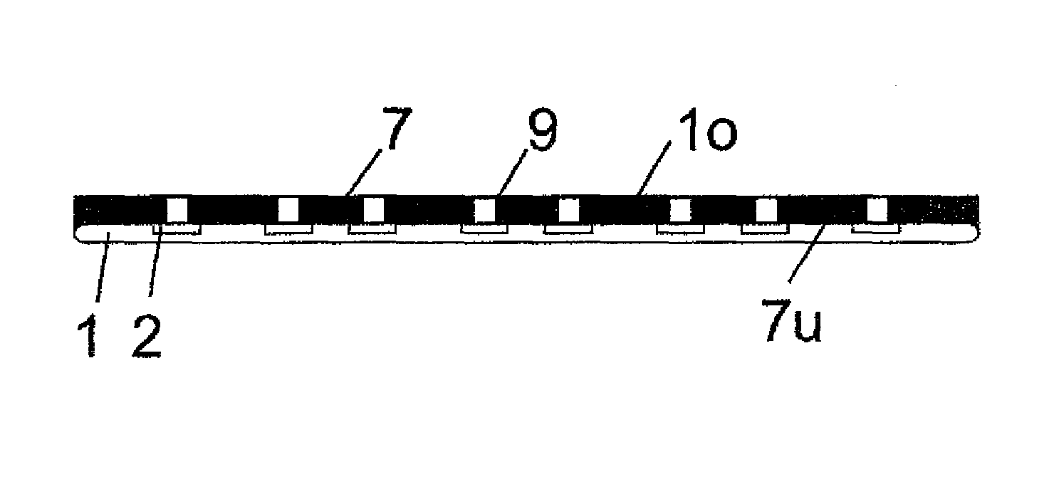
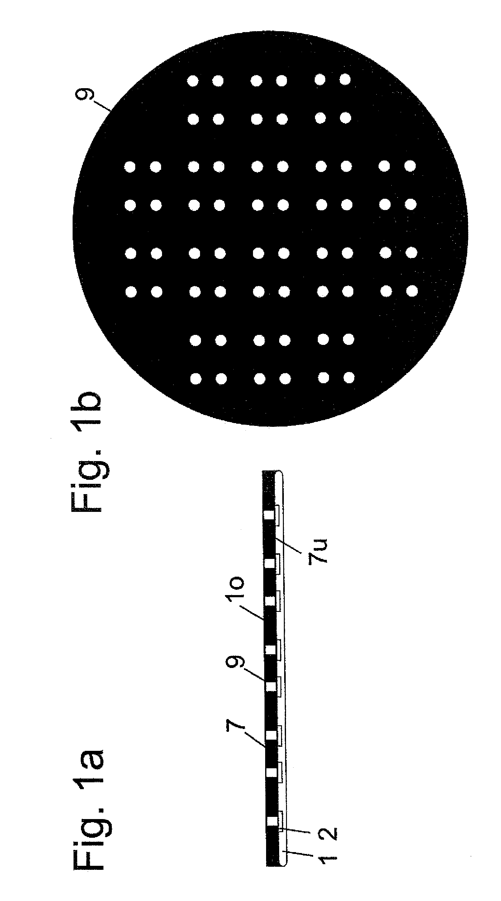
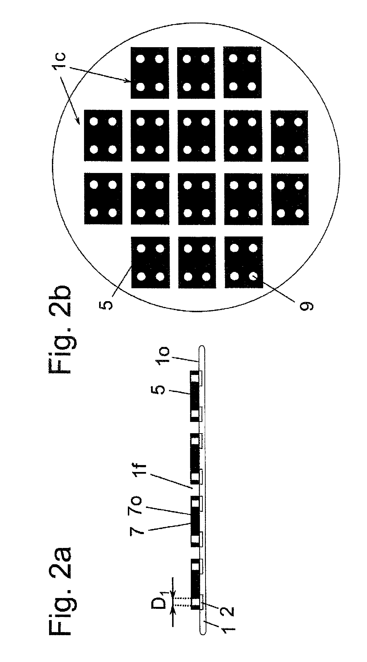
[0037]In the method step which is shown in FIGS. 1a and 1b, a function layer 7 with low elasticity (therefore provided with a high modulus of elasticity) is applied to a surface 10 of the substrate. Especially spin coating, spray coating, extrusion coating, lamination, gas precipitation or similar methods are used for application. The function layer 7 is used as underfill or support material for supporting the chips 4 which are tacked onto the substrate 1 by the method of the present invention.

[0038]The function layer 7 is applied over the entire surface and is already solid or rigid upon application or at least at the end of the application process or is transferred into a solid or rigid state by phase conversion or a polymerization step. A photostructuring process uncovers (i.e., removes) the function layer 7 at the contact-making positions, at which there are contacts 2 on the surface 1o so that from one chip contact side 7o facing away from the surface 1o to the surface 1o a fre...


PUM


Abstract

A method for tacking of chips onto a substrate at chip positions which are distributed on a surface of the substrate. The method includes the following steps: formation or application of a function layer onto the substrate, removing the function layer from the substrate at the chip positions at least in the region of contacts to uncover the contacts, tacking chips onto one chip contact side of the function layer at the chip positions and contacting the chips with the contacts via contact elements.

Description

FIELD OF THE INVENTION[0001]This invention relates to a method for tacking of chips onto a substrate at chip positions which are distributed on a surface of the substrate.BACKGROUND OF THE INVENTION[0002]Chips are often joined via bumps to bond pads embedded in a substrate, therefore electrically conductive contacts. To bridge the distance between the chips and the substrate and to produce a mechanical connection between the chip and the substrate, underfill materials are used which are also employed for mechanical relief of the bumps from the chip or substrate. The underfill material increases the service life of the chips several-fold. Mainly the fatigue strength of the bond connection at complete stress reversal with respect to temperature changes and / or mechanical loads is increased.[0003]In practice an underfill material with low viscosity is placed between the chips and the substrate by capillary action after the underfill material has been applied for example by inkjet method...

Claims


Application Information

Patent Timeline
Patent Type & Authority Patents(United States)
IPC IPC(8): H01L21/00H01L23/00H01L21/56H01L25/00H01L25/065
CPCH01L24/97H01L21/563H01L24/27H01L24/29H01L24/73H01L24/81H01L24/83H01L24/92H01L24/13H01L25/0655H01L25/50H01L2224/131H01L2224/13013H01L2224/13014H01L2224/2741H01L2224/27416H01L2224/27418H01L2224/27436H01L2224/27444H01L2224/27515H01L2224/27622H01L2224/29011H01L2224/29012H01L2224/2919H01L2224/73104H01L2224/73153H01L2224/73204H01L2224/8114H01L2224/81191H01L2224/81192H01L2224/81193H01L2224/81203H01L2224/81815H01L2224/81907H01L2224/83002H01L2224/83009H01L2224/83102H01L2224/83192H01L2224/83193H01L2224/83203H01L2224/83856H01L2224/83907H01L2224/9205H01L2224/9211H01L2224/97H01L2924/181H01L2924/381H01L2924/00014H01L2224/81H01L2224/83H01L2924/00015H01L2224/16225H01L2224/32225H01L2924/00012H01L2924/00
Inventor BURGGRAF, JURGENWIMPLINGER, MARKUSWIESBAUER, HARALDSIGL, ALFRED
Owner EV GRP E THALLNER GMBH
Why Eureka
Try Eureka