Method of semiconductor device including step of cutting substrate at opening of insulating layer

a technology of semiconductor devices and insulating layers, applied in the direction of semiconductor devices, electrical devices, transistors, etc., can solve the problems of affecting the production efficiency of semiconductor devices. , to achieve the effect of reducing defects and high productivity

Active Publication Date: 2016-02-09
SEMICON ENERGY LAB CO LTD
View PDF36 Cites 10 Cited by
  • Summary
  • Abstract
  • Description
  • Claims
  • Application Information

AI Technical Summary

Benefits of technology

[0011]In the case where peeling is performed between a peeling layer provided over a substrate and a layer to be peeled (hereinafter referred to as layer) formed over the peeling layer, a stack formed of thin films (e.g., the layer, a thin film transistor (TFT), a wiring, and an interlayer film) is provided over the peeling layer. The stack has a thickness of several micrometers or less and is very fragile. When peeling is performed between the peeling layer and the layer, a high bending stress is applied to an end portion of the layer (a peeling starting point); as a result, breaking or cracking (hereinafter, collectively referred to as crack) easily occurs in the layer. Moreover, when such a crack develops from the end portion of the layer into a semiconductor element or a light-emitting element, these elements might be broken.
[0012]To improve productivity of flexible devices, it is preferable that a plurality of devices be manufactured at a time over a large substrate and the substrate be divided with a scriber or the like. This step causes a problem in that a crack occurs in or develops from an end portion of the substrate due to stress applied when the substrate is divided.
[0013]In view of the above, an object of one embodiment of the present invention is to provide a flexible device with fewer defects caused by a crack. Another object is to provide a flexible device having high productivity.
[0021]The present invention can provide a flexible device with fewer defects caused by a crack or a flexible device having high productivity.

Problems solved by technology

The stack has a thickness of several micrometers or less and is very fragile.
Moreover, when such a crack develops from the end portion of the layer into a semiconductor element or a light-emitting element, these elements might be broken.
This step causes a problem in that a crack occurs in or develops from an end portion of the substrate due to stress applied when the substrate is divided.

Method used


Image

  • Method of semiconductor device including step of cutting substrate at opening of insulating layer
  • Method of semiconductor device including step of cutting substrate at opening of insulating layer
  • Method of semiconductor device including step of cutting substrate at opening of insulating layer

Examples


embodiment 1

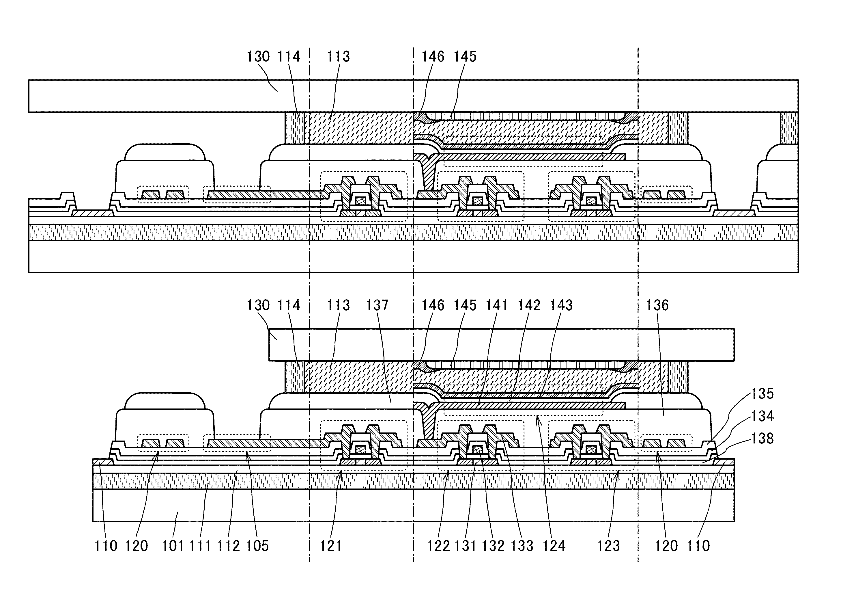
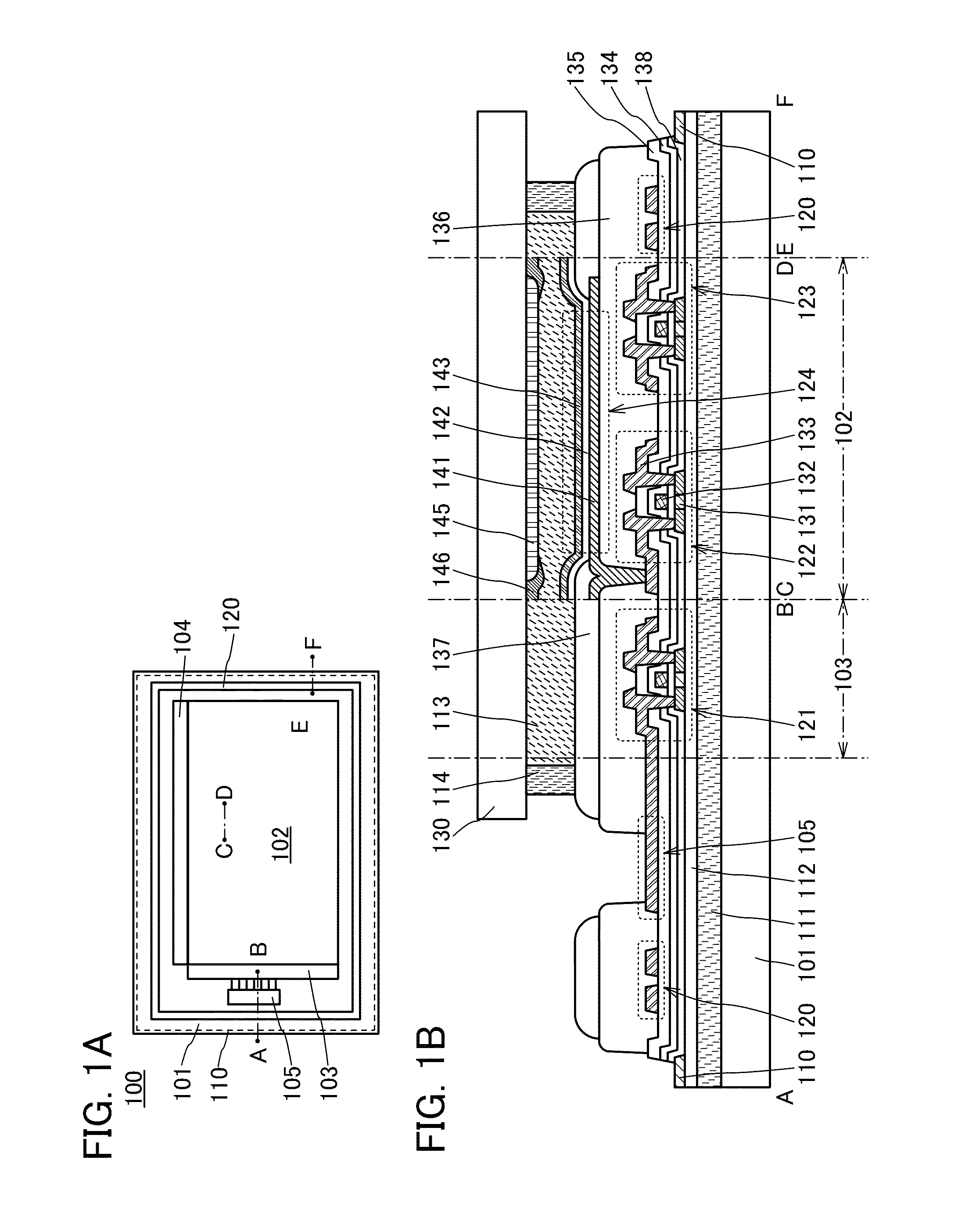
[0038]In this embodiment, a structure and a manufacturing method of an image display device, which is an example of a semiconductor device of one embodiment of the present invention, are described with reference to drawings. As an example of the image display device, an image display device (hereinafter, also referred to as display device) including an organic EL element is described below.

[0039]Note that in this specification and the like, the display device may include any of the following modules in its category: a module in which a connector such as a flexible printed circuit (FPC) or a tape carrier package (TCP) is attached to a display device; a module having a TCP provided with a printed wiring board at the end thereof; a module having an integrated circuit (IC) directly mounted over a substrate over which a display element is formed by a chip on glass (COG) method; a module in which a touch sensor is mounted.

[Structural Example of Display Device]

[0040]FIG. 1A is a schematic ...

embodiment 2

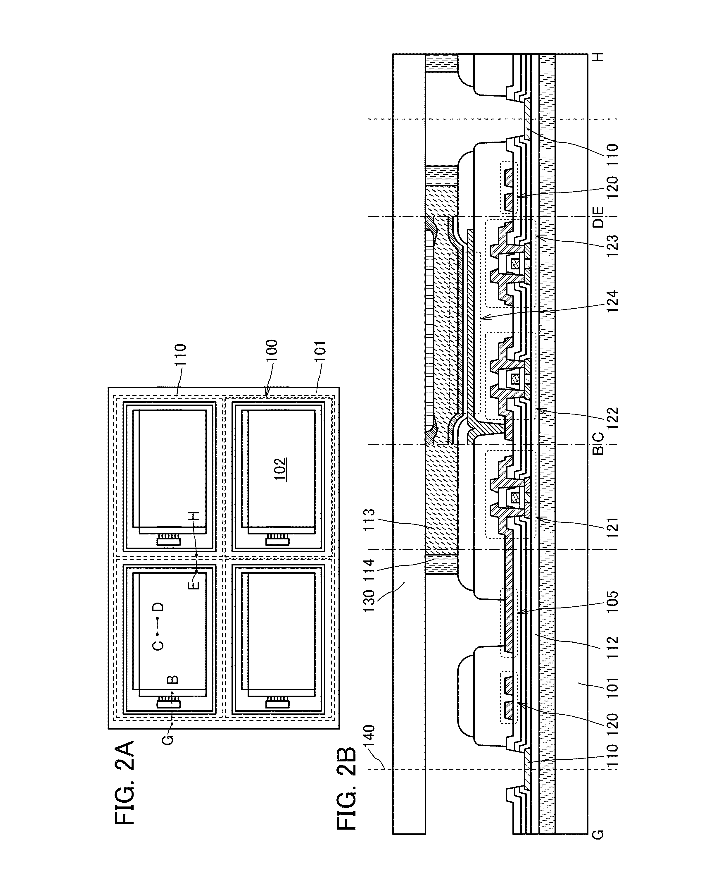
[0193]In this embodiment, a structure of a display device that differs from the display device shown in Embodiment 1 is described as an example. Note that description of the portions described in Embodiment 1 is omitted.

[Structural Example]

[0194]An example of a structure of an image display device in which a liquid crystal element is used as a display element is described below.

[0195]FIG. 7 is a schematic cross-sectional view of a display device 200. The display device 200 differs from the display device 100 described in Embodiment 1 mainly in that a liquid crystal element is used as a display element and a transistor has a different structure.

[0196]The display portion 102 includes a liquid crystal element 224 using an in-plane switching (IPS) mode. In the liquid crystal element 224, the orientation of a liquid crystal is controlled by an electric field generated in a direction parallel to the substrate surface.

[0197]A pixel includes at least one switching transistor 222 and a stora...

embodiment 3

[0212]In this embodiment, electronic devices each including a display device are described as examples of a semiconductor device of one embodiment of the present invention.

[0213]The display device of one embodiment of the present invention has a bendable display surface. Examples of such a display device include a television set (also referred to as television or television receiver), a monitor of a computer, a camera such as a digital camera or a digital video camera, a digital photo frame, a mobile phone set (also referred to as mobile phone or mobile phone device), a portable game machine, a portable information terminal, an audio reproducing device, and a large game machine such as a pachinko machine. In addition, a lighting device or a display device can be incorporated along a curved inside / outside wall surface of a house or a building or a curved interior / exterior surface of a car. In addition, a lighting device or a display device can be incorporated along a curved inside / ou...


PUM


Abstract

Provided is a flexible device with fewer defects caused by a crack or a flexible device having high productivity. A semiconductor device including: a display portion over a flexible substrate, including a transistor and a display element; a semiconductor layer surrounding the display portion; and an insulating layer over the transistor and the semiconductor layer. When seen in a direction perpendicular to a surface of the flexible substrate, an end portion of the substrate is substantially aligned with an end portion of the semiconductor layer, and an end portion of the insulating layer is positioned over the semiconductor layer.

Description

BACKGROUND OF THE INVENTION[0001]1. Field of the Invention[0002]The present invention relates to a semiconductor device.[0003]The “semiconductor device” in this specification and the like means all devices that can operate by utilizing semiconductor characteristics. Accordingly, a transistor, a semiconductor element, a semiconductor circuit, a memory device, an imaging device, an electro-optical device, a power generation device (e.g., a thin film solar cell and an organic thin film solar cell), an electronic device, and the like are included in the category of the semiconductor device.[0004]2. Description of the Related Art[0005]In recent years, a flexible device in which a semiconductor element, a light-emitting element, and the like are provided over a flexible substrate has been developed. Typical examples of the flexible device include, as well as a lighting device and an image display device, a variety of semiconductor circuits including a semiconductor element such as a trans...

Claims


Application Information

Patent Timeline
Patent Type & Authority Patents(United States)
IPC IPC(8): H01L21/84H01L29/786H01L27/12
CPCH01L29/78606H01L21/84H01L27/1218H01L27/1262H01L27/1266H01L27/1222H01L2021/775H01L29/78603
Inventor ADACHI, HIROKIKUMAKURA, KAYO
Owner SEMICON ENERGY LAB CO LTD
Why Eureka
Try Eureka