Tunable SOI laser

a silicononinsulator and wavelength technology, applied in semiconductor lasers, instruments, optical elements, etc., can solve the problems of insufficient application, low efficiency, and high cost of manufacturing, and achieve the effect of reducing the distance between p and p, reducing the cost of manufacturing, and reducing the cost of production

Active Publication Date: 2016-02-23
ROCKLEY PHOTONICS LTD
View PDF48 Cites 16 Cited by
  • Summary
  • Abstract
  • Description
  • Claims
  • Application Information

AI Technical Summary

Benefits of technology

[0015]Preferably, a mirror of the laser cavity is located at the back end of the semiconductor gain medium. In this way, there is only one gain medium-SOI waveguide interface (i.e. that located at the front end of the gain medium). As a result, the tunable laser of the present invention has an improved power efficiency because the optical losses associated with coupling between the semiconductor gain medium and the waveguide platform are significantly reduced. In addition, the manufacturing complexity is reduced as it is only necessary to align the front end of the gain medium during manufacturing, for example in a flip-chip process.
[0140]Where a waveguide platform is bifurcated, a transition is optionally located between the point at which the waveguide platform is coupled to the semiconductor gain medium and the point at which the two bifurcated arms are coupled. In this way, the height (and / or width) of the waveguide is maximised at a first height (and / or width) in the gain medium but the height (and / or width) is minimised at a second height (and / or width) at the arm of the bifurcated waveguide platform where the Fabry-Perot filters are located. In alternative embodiments, a transition region may be located after the bifurcation.

Problems solved by technology

However, they are expensive to manufacture as a result of the need for multiple epitaxial re-growth steps.
To date, demonstrations have been relatively slow to tune, making them inadequate for certain applications.
Of course, the major challenge for SOI photonic integrated platforms is the fact that silicon is not an optical gain medium and does not therefore form an ideal medium for photonic circuits incorporating lasers.
One drawback of such a design is the high optical power loss, particularly due to coupling between the waveguides formed from the silicon substrate and any waveguides in optical devices placed in, grown onto, or otherwise incorporated into the platform.

Method used


Image

  • Tunable SOI laser
  • Tunable SOI laser
  • Tunable SOI laser

Examples


Embodiment Construction

[0161]Embodiments of the present invention which relate to SOI lasers including multimode interference devices are described below with reference to FIGS. 1 to 5.

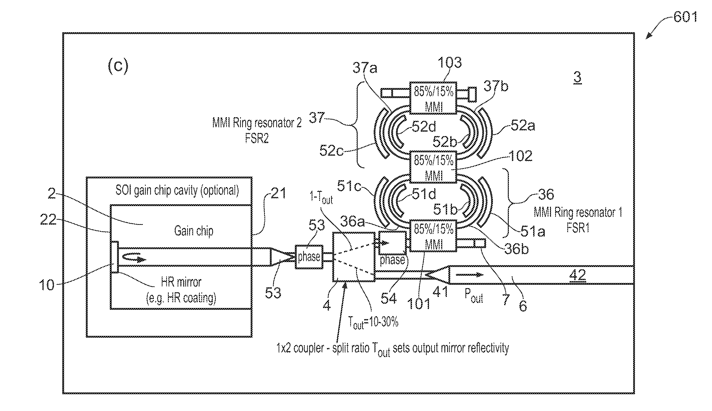
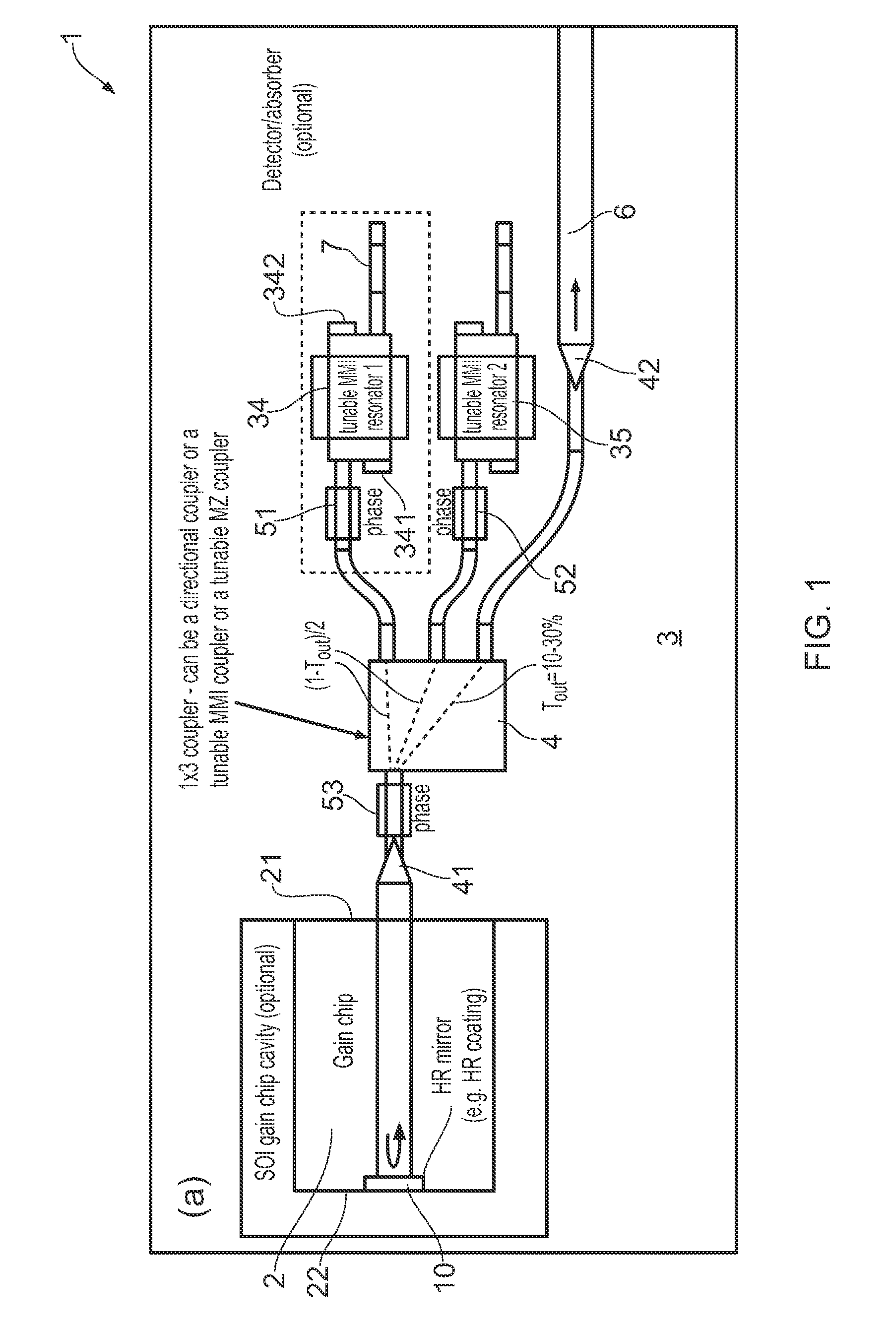
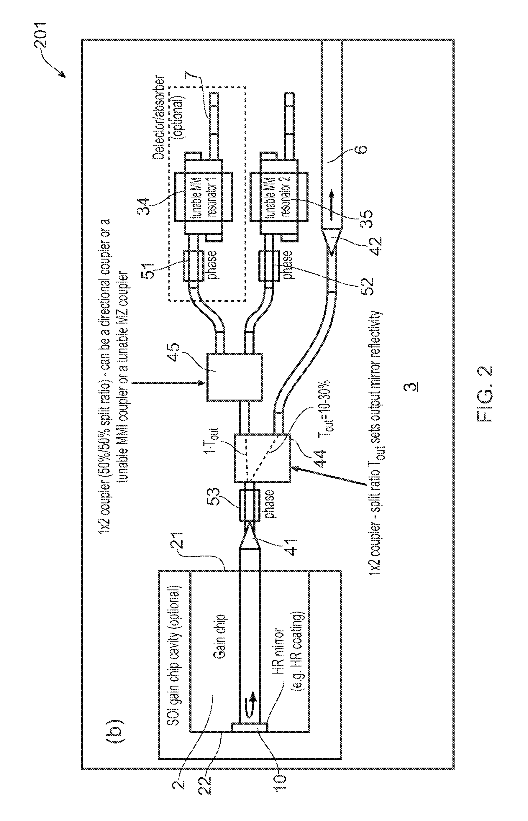
[0162]Referring to FIG. 1, a wavelength tunable silicon-on-insulator (SOI) laser is shown, the laser having a laser cavity which is made up of a semiconductor gain medium, 2 and a phase-tunable waveguide platform, 3 coupled to the front end of the semiconductor gain medium. In the embodiment shown in FIG. 1, the semiconductor gain medium, 2 takes the form of a gain chip and the gain chip shown is located inside of an SOI gain chip cavity.

[0163]The phase-tunable waveguide platform includes a first multimode interference (MMI) device (MMI resonator device) 34 (as shown in FIG. 3), and a second MMI device (MMI resonator device), 35 in a parallel arrangement. Each MMI device includes a multi-mode waveguide; a first reflective surface, 341 partially covering one end of the multimode waveguide; and a second reflective surface, 34...


PUM


Abstract

A wavelength tunable silicon-on-insulator (SOI) laser comprising: a laser cavity including: a semiconductor gain medium having a front end and a back end, wherein a mirror of the laser cavity is located at the back end of the semiconductor gain medium; and a phase-tunable waveguide platform coupled to the front end of the semiconductor gain medium, the phase-tunable waveguide platform comprising: a first resonator and a second resonator; at least one resonator being a phase-tunable resonator; wherein the first resonator is any one of: an MMI device including a pair of reflective surfaces defining a resonator cavity therebetween such that the device is configured to act as a Fabry-Perot filter; a ring resonator; or a waveguide Fabry-Perot filter; and wherein the second resonator is any one of: an MMI device including a pair of reflective surfaces defining a resonator cavity therebetween such that the device is configured to act as a Fabry-Perot filter; a ring resonator; or a waveguide Fabry-Perot filter.

Description

FIELD OF THE INVENTION[0001]The present invention relates to a wavelength tunable silicon-on-insulator (SOI) laser having a phase-tunable waveguide platform comprising a first resonator device and a second resonator device.BACKGROUND OF THE INVENTION[0002]Tunable semiconductor lasers are often used for applications in which an occasional but precise tuning of wavelength is required. They can provide excellent wavelength stability and are typically manufactured as monolithic photonic integrated circuits (PICs) in a gain medium such as a III-V semiconductor material. However, they are expensive to manufacture as a result of the need for multiple epitaxial re-growth steps. To date, demonstrations have been relatively slow to tune, making them inadequate for certain applications.[0003]Particularly in applications where the precise wavelength of the laser is not so important, there is a need for tunable lasers with a wide tuning range (>30 nm) but with fast switching speeds (of less t...

Claims


Application Information

Patent Timeline
Patent Type & Authority Patents(United States)
IPC IPC(8): H01S3/10H01S5/10H01S5/125H01S5/02H01S5/14H01S3/08H01S3/106H01S5/12G02B6/12H01S3/105H01S3/083H01S5/028
CPCH01S3/1062H01S3/083H01S3/08027H01S3/10053H01S5/021H01S5/1007H01S5/1071H01S5/125H01S5/14H01S5/142G02B6/12007H01S3/105H01S3/106H01S5/028H01S5/1209H01S5/141H01S2301/03H01S5/1003H01S5/1032H01S5/0237H01S5/02325G02B6/1228G02B6/29343G02F1/225H01S5/06H01S5/10
Inventor RICKMAN, ANDREWZILKIE, AARON JOHN
Owner ROCKLEY PHOTONICS LTD
Why Eureka
Try Eureka