
MEMS devices anti-stiction coating and encapsulant having opposing water resitive characteristics

a technology of anti-stiction coating and encapsulation, which is applied in the direction of coating, microstructural device, microstructural device, etc., can solve the problems of affecting the performance of the mems sensor or transducer located within the mems device, and disclose the way to protect the mems devi

Active Publication Date: 2016-03-15
PANASONIC CORP
View PDF2 Cites 5 Cited by
  • Summary
  • Abstract
  • Description
  • Claims
  • Application Information

AI Technical Summary

Benefits of technology

The patent is about a technique for packaging MEMS devices that allows them to sense rotational information while being isolated from external stress, strain, vibration, shock, and thermal transients. The technique involves using interposing materials that permit mechanical, thermal, and vibrational isolation of the transducer from the substrate, while still permitting electrical continuity between them. This results in increased isolation from both external and internal stimuli that are not desirable, reducing noise. The method also involves customizing the location of voids / air cavity / environmental isolations inside the MEMS device package by treating the surfaces with anti-stiction coatings to create air cavity by the tendency of nonpolar substances to aggregate in aqueous solution and exclude water molecules. The addition of material / encapsulant / mold applies a compressive stress to all objects encased in it, shielding the MEMS device from external environmental factors. This technique allows for predictable performance and amenable to electronic controls.

Problems solved by technology

External forces transmitted from the housing structure to the MEMS device may detrimentally affect the performance of the MEMS sensor or transducer located within the MEMS device.
While certain prior publications address how to protect MEMS devices with sensing gaps on the order of micrometers, they have not disclosed how to protect MEMS devices wherein the sensing gaps are on the order of nanometers.
When this gap distance is affected by stimuli other than the desired signal source, it is perceived as “noise” and is consequently undesirable.

Method used


Image

  • MEMS devices anti-stiction coating and encapsulant having opposing water resitive characteristics
  • MEMS devices anti-stiction coating and encapsulant having opposing water resitive characteristics
  • MEMS devices anti-stiction coating and encapsulant having opposing water resitive characteristics

Examples


Embodiment Construction

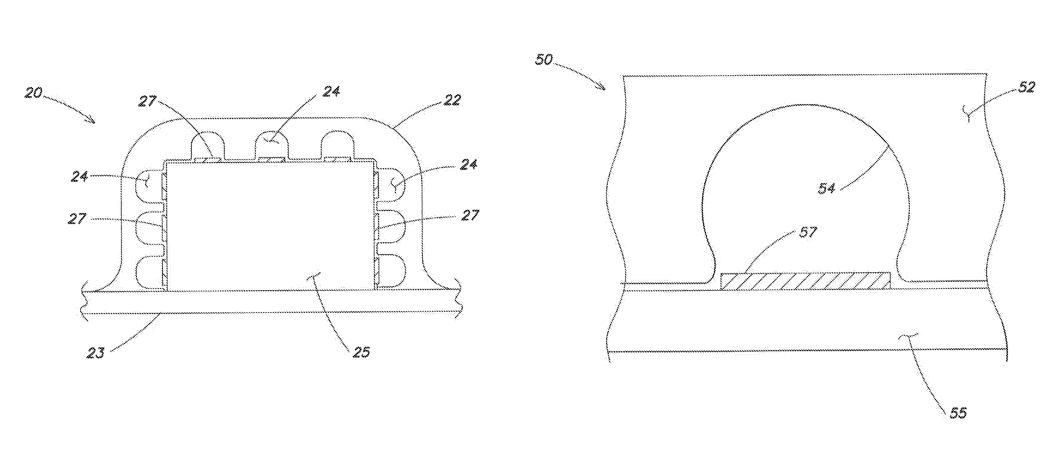
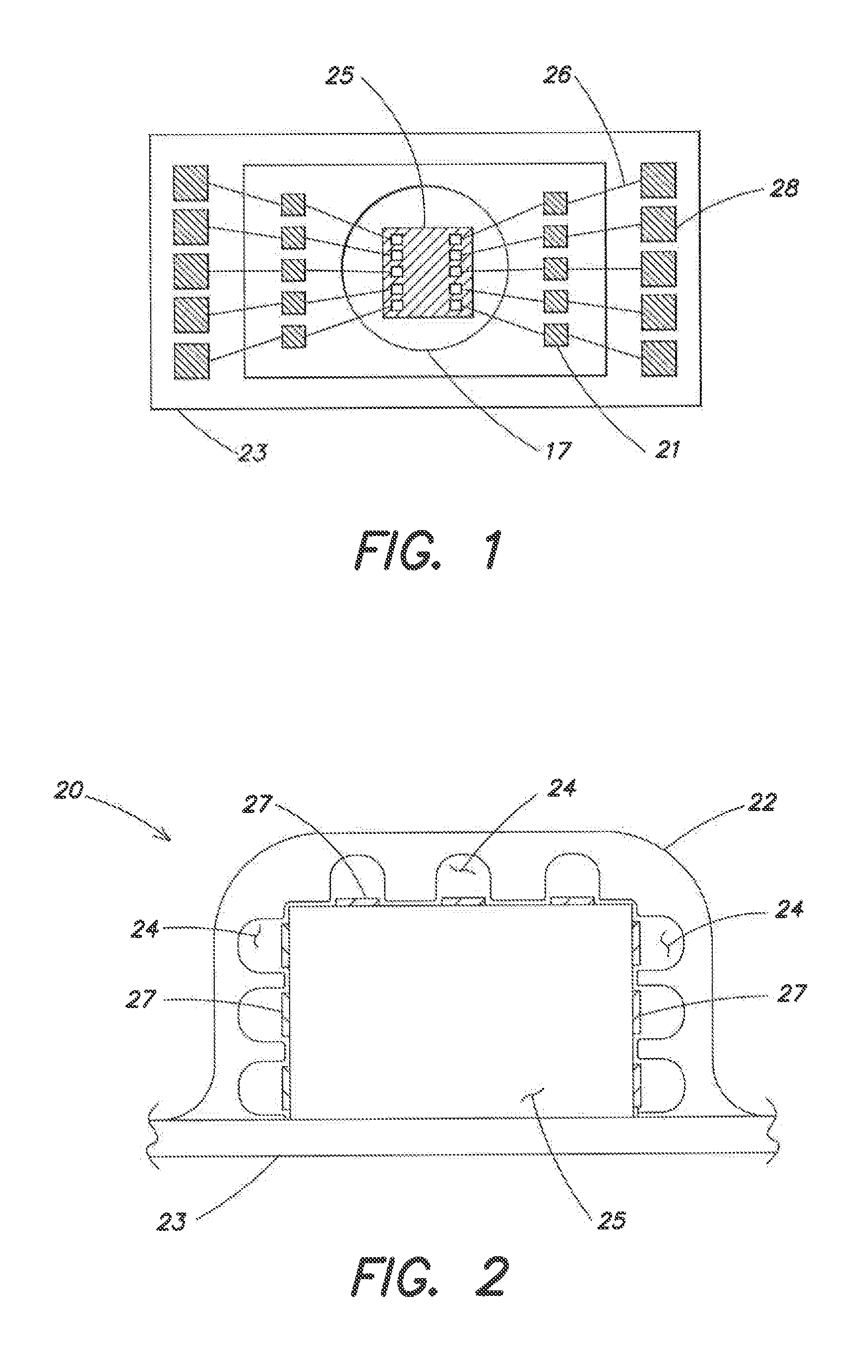
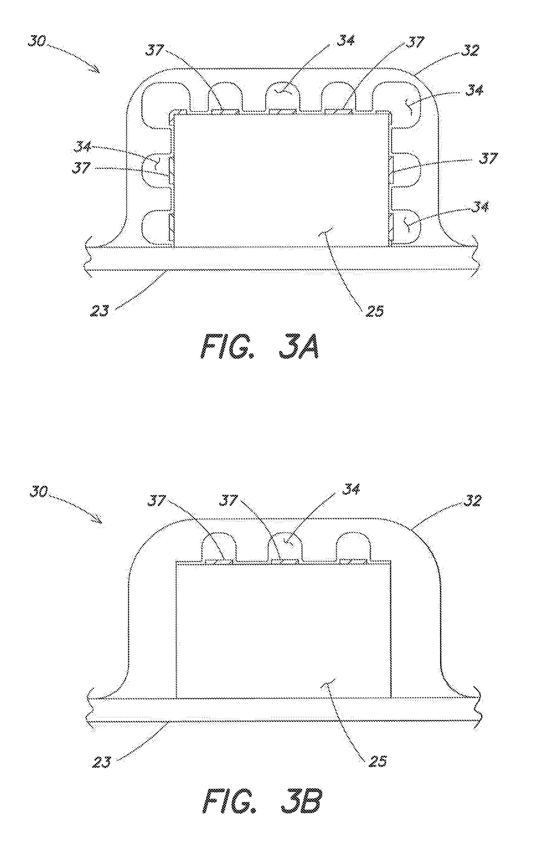
[0019]MEMS devices, in particular capacitive devices like gyroscopes, accelerometers, microphones, pressure sensors and combinations thereof, are susceptible to having their performance compromised by externally induced strains. This is due, in part, because there are typically very small air gaps, on the order of 100's of nanometers in BAW devices, and micrometers in other devices, that will change when then the structures defining them are moved with respect to each other. The external strains may be introduced by a number of methods. One for example is the thermal mismatch between the device and the board to which it is mounted and also the solder or adhesive used to achieve such attachment. Such mismatch results in a warpage of the MEMS package, and, hence, an induced strain in all bodies in the system. Another source of strain is that which is incurred during the assembly of the MEMS device. In this scenario, the MEMS sensor, and the surrounding housing / package, along with adhe...


PUM

PropertyMeasurementUnit
Hydrophilicityaaaaaaaaaa
Hydrophobicityaaaaaaaaaa
Stress optical coefficientaaaaaaaaaa

Abstract

Disclosed is an isolation mechanism and technique for packaging a MEMS transducer, such as a bulk acoustic wave gyroscope or accelerometer, to provide isolation from externally applied (or internally induced) stress, strain, vibration, shock and thermal transients. The disclosed methods and techniques enable the location of voids / air cavity / environmental isolations inside an encapsulant or over mold compound to be custom selected by treating at least a portion of the exterior surfaces of the MEMS device package with anti-stiction coatings to create opposing hydrophobic and hydrophilic conditions which during encapsulant and transfer molding steps create voids or air bubbles in the proximity of the anti-stiction coating due to the opposing water resistive characteristic of encapsulant.

Description

FIELD OF THE INVENTION[0001]The disclosure relates to Microelectromechanical Systems (MEMS) devices, and, more specifically, to an apparatus and technique for isolating MEMS devices from external and internal stimuli.BACKGROUND OF THE DISCLOSURE[0002]Microelectromechanical Systems (MEMS) devices are typically attached to a housing structure, and the housing structure attached to another entity, such as a circuit board. External forces transmitted from the housing structure to the MEMS device may detrimentally affect the performance of the MEMS sensor or transducer located within the MEMS device. For example, if the sensor 30 comprises a bulk acoustic wave resonator having a disc shaped resonator element, such as disclosed in United States Patent Application Publication 2012 / 0227,487, the transducer may be supported at the disc center by an anchor. For other devices utilizing a capacitive resonator element, such as those disclosed in U.S. Pat. No. 7,023,065, an anchor may still suppo...

Claims


Application Information

Patent Timeline
IPC IPC(8): B81B3/00B81C1/00
CPCB81B3/0018B81C1/00182B81B3/0035B81B3/0005B81C1/0019B81B3/0072B81C1/00277B81B7/0077B81C2203/0136
Inventor SHAH, ASHISH, A.
Owner PANASONIC CORP
Learn More