Method for reducing particle generation at bevel portion of substrate

a technology of bevel portion and substrate, which is applied in the field of transporting substrates, can solve the problems of serious yield reduction, film easily peeling off from the substrate surface, and micro particle generation at the edge of the substrate, and achieves the effects of reducing micro particles, high mechanical strength, and high mechanical strength

Active Publication Date: 2016-05-17
ASM IP HLDG BV
View PDF1 Cites 326 Cited by
  • Summary
  • Abstract
  • Description
  • Claims
  • Application Information

AI Technical Summary

Benefits of technology

[0007]Some embodiments provide a method to reduce micro particles generated by mechanical clamping or contact when clamping a substrate edge for transfer. In some embodiments, particle generation at the edge of a substrate is inhibited by depositing a film having high mechanical strength by generating a plasma only over the substrate edge area (bevel portion) which has no influence on the device processing area of the substrate. Typically, depositing a film having high mechanical strength on the bevel portion can cancel mechanical stress generated in the underlying layers. The deposition can be accomplished in a single step performed selectively and exclusively on the edge area (bevel portion), thereby inhibiting particle generation caused by edge clamping or mechanical contact during subsequent substrate transfer steps.

Problems solved by technology

In semiconductor or liquid crystal display (LCD) manufacturing, micro particle generation which occurs at substrate edges is a serious concern.
This problem most likely occurs when the film having tensile mechanical stress (“tensile film”) is deposited on the substrate surface, which film easily peels off from the substrate surface.
After these particles generated at the edge of the substrate are detached from the substrate surface, they move over the surface and adhere to the substrate surface, causing electrical damage to a highly integrated circuit and leading to serious yield reduction.
However, this device cannot be adapted to transfer a substrate under a vacuum environment.
For these reasons, the vacuum chuck method does not meet the requirements for highly integrated modern semiconductor manufacturing.
This measure, however, increases the overall substrate transfer time and leads to a serious problem of low productivity.

Method used


Image

  • Method for reducing particle generation at bevel portion of substrate
  • Method for reducing particle generation at bevel portion of substrate
  • Method for reducing particle generation at bevel portion of substrate

Examples


example

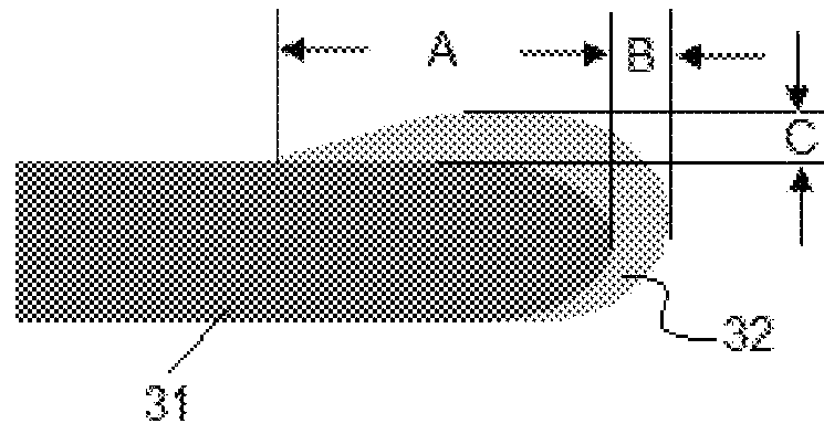
[0050]A compressive bevel film (silicon nitride film) is formed on a substrate (Φ300 mm) having an underlying film (amorphous carbon) by PECVD under the conditions shown below using the PECVD apparatus illustrated in FIG. 3, wherein a distance between the upper and lower electrodes is 15 mm at the peripheries of the upper and lower electrodes, and 1.5 mm in an inner area surrounded by the peripheries. The maximum thickness of the bevel film is 50 nm.

[0051]

TABLE 2(the numbers are approximate)PrecursorSiH4 at a flow rate of 100 sccmAdditive gasNH3 at a flow rate of 500 sccmInert gasN2 at a flow rate of 5,000 sccm, and He at aflow rate of 500 sccmProcess temperature380° C.Process pressure400 PaProcess duration8 secondsRF power13.56 MHz at 600 W and 400 kHz at 400 W

[0052]FIG. 9 is a graph showing the thickness distribution of the film deposited on the substrate. As shown in FIG. 9, the bevel film has a maximum thickness at the tip of the substrate and becomes thinner toward the center o...


PUM

PropertyMeasurementUnit
diameteraaaaaaaaaa
thicknessaaaaaaaaaa
thicknessaaaaaaaaaa

Abstract

A method for transporting a substrate using an end effector which mechanically clamps a periphery of the substrate includes: before transporting the substrate, depositing a compressive film only on, at, or in a bevel portion of the substrate; and transporting the substrate whose bevel portion is covered by the compressive film as the outermost film, using an end effector while mechanically clamping the periphery of the substrate.

Description

BACKGROUND OF THE INVENTION[0001]1. Field of the Invention[0002]The present invention generally relates to transportation of a substrate using an end effector which mechanically clamps the periphery of the substrate, in particular, to a method for reducing particle generation at a bevel portion of the substrate during the transportation.[0003]2. Description of the Related Art[0004]In semiconductor or liquid crystal display (LCD) manufacturing, micro particle generation which occurs at substrate edges is a serious concern. Micro particles are generated when the edge of a substrate such as a Si wafer is scratched by a clamping device of a substrate transfer robot to mechanically clamp the edge of the substrate. Also, when a film deposited on a substrate edge surface is scratched by a clamp and partially peeled, micro particles are generated. This problem most likely occurs when the film having tensile mechanical stress (“tensile film”) is deposited on the substrate surface, which film...

Claims


Application Information

Patent Timeline
Patent Type & Authority Patents(United States)
IPC IPC(8): H01L23/31H01L21/677C23C16/458C23C16/04B25J11/00H01J37/32C23C16/50H01L21/67
CPCH01L21/67742B25J11/0095C23C16/04C23C16/4585C23C16/50H01J37/32532H01J37/32541H01L21/67011H01L23/3171H01L23/3185H01J37/32091H01J37/32385H01L21/68707C23C16/345C23C16/4401C23C16/505H01L2924/0002H01L2924/00
Inventor MORI, YUKIHIRO
Owner ASM IP HLDG BV
Why Eureka
Try Eureka