Apparatus and methods for micro-transfer-printing

a technology of micro-transfer printing and apparatus, applied in the field of micro-transfer printing apparatus, can solve the problems of sagging between posts, compression of the transfer device, and difficulty in picking up and placing ultra-thin and/or small devices using this technology, and achieves the effects of increasing the initial acceleration, high acceleration, and high velocities

Active Publication Date: 2016-06-07
X DISPLAY CO TECH LTD
View PDF107 Cites 122 Cited by
  • Summary
  • Abstract
  • Description
  • Claims
  • Application Information

AI Technical Summary

Benefits of technology

[0011]As described herein, the present disclosure provides methods and tools for micro transfer printing. In certain embodiments, the disclosed technology utilizes high acceleration when picking up chips from the source wafer. Traditional methods of the “pick” process utilize a vertical stage (with stamp attached) that moves the stamp rapidly upward, away from the substrate. Typically, approximately 1 g of acceleration is used to pick up devices from the native substrate. In certain embodiments, it is advantageous to increase the initial acceleration (5-100 g) to achieve higher velocities during the pick process. The velocity at separation occurs at very small travel distances that are dependent on the compression of the stamp at lamination. Higher acceleration can create higher separation velocities at small distances that in turn increases the adhesion between the stamp and source. Movement of the stamp in the downward direction, away from the source substrate, during the “pick” process can increase the overall acceleration by moving with gravity, and therefore can add an additional 1 g of acceleration to the transfer.
[0012]In certain embodiments, heat-assisted micro-transfer-printing is performed to adhesiveless surfaces and topographic surfaces. Polymer encapsulations can be used to enhance transfer of semiconductor devices to non-native substrates when the polymer is designed to contract and then reflow while in contact with the destination substrate. The polymer layer can be subsequently removed while leaving behind the transferred device on the non-native substrate. This also improves the ability to micro-transfer-print to topographic surfaces.

Problems solved by technology

It is often difficult to pick up and place ultra-thin and / or small devices using this technology.
However, compression of the transfer device poses several issues.
Among other things, there is a possibility of sagging between posts.
As the span between adjacent posts is increased, the risk of sag causing problems increases.

Method used


Image

  • Apparatus and methods for micro-transfer-printing
  • Apparatus and methods for micro-transfer-printing
  • Apparatus and methods for micro-transfer-printing

Examples


Embodiment Construction

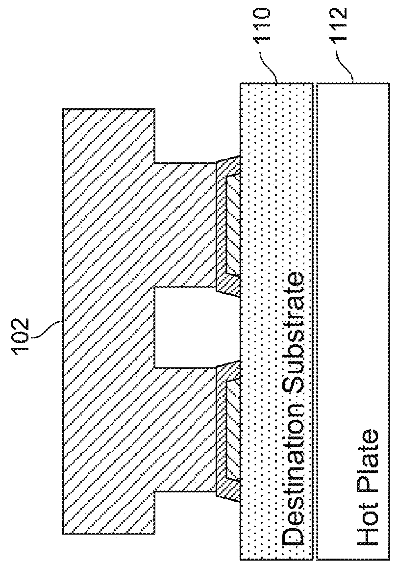
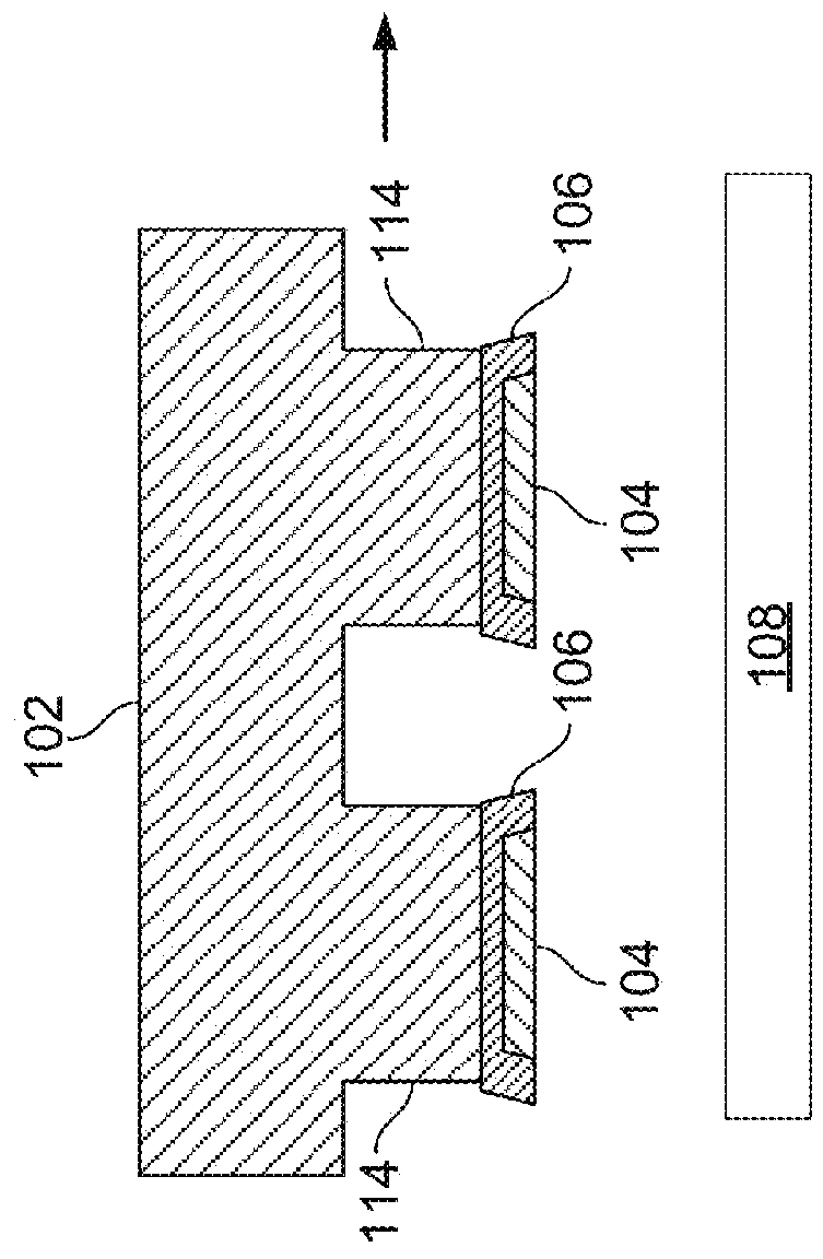
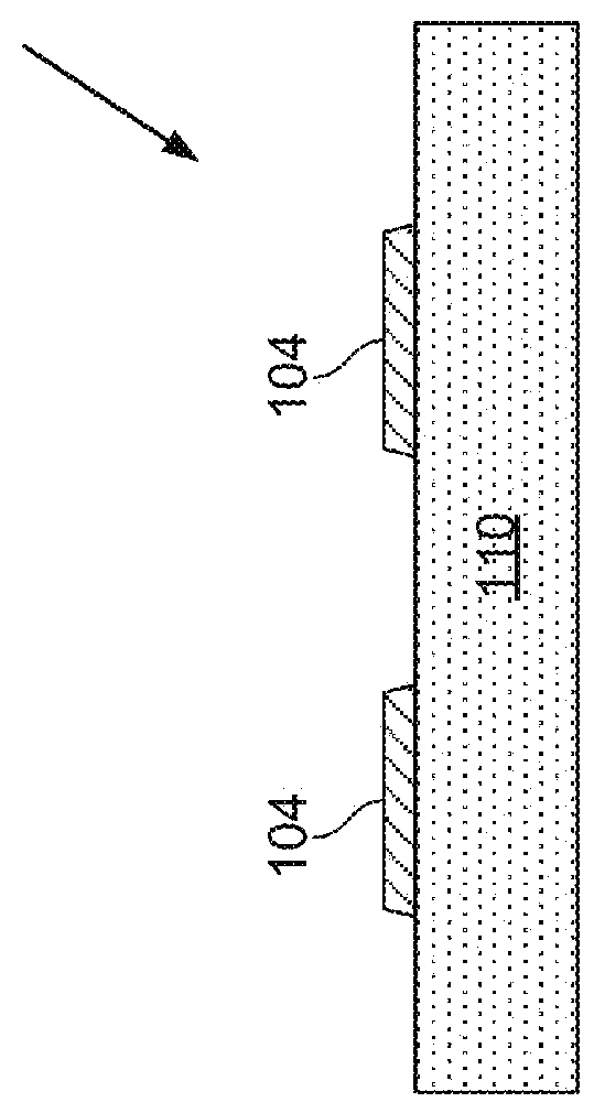
[0335]As used herein the expression “semiconductor element” and “semiconductor structure” are used synonymously and broadly refer to a semiconductor material, structure, device, or component of a device. Semiconductor elements include high-quality single crystalline and polycrystalline semiconductors, semiconductor materials fabricated via high-temperature processing, doped semiconductor materials, organic and inorganic semiconductors, and composite semiconductor materials and structures having one or more additional semiconductor components or non-semiconductor components, such as dielectric layers or materials or conducting layers or materials. Semiconductor elements include semiconductor devices and device components including, but not limited to, transistors, photovoltaics including solar cells, diodes, light-emitting diodes, lasers, p-n junctions, photodiodes, integrated circuits, and sensors. In addition, semiconductor element can refer to a part or portion that forms a functi...


PUM


Abstract

In an aspect, a system and method for assembling a semiconductor device on a receiving surface of a destination substrate is disclosed. In another aspect, a system and method for assembling a semiconductor device on a destination substrate with topographic features is disclosed. In another aspect, a gravity-assisted separation system and method for printing semiconductor device is disclosed. In another aspect, various features of a transfer device for printing semiconductor devices are disclosed.

Description

PRIORITY APPLICATIONS[0001]This application claims priority to and the benefit of U.S. Provisional Patent Application No. 62 / 026,694, filed Jul. 20, 2014, entitled “Apparatus and Method for Micro-Transfer Printing” and U.S. Provisional Patent Application No. 62 / 027,166, filed Jul. 21, 2014, entitled “Methods and Tools for Micro-Transfer Printing,” the contents of each of which is incorporated by reference herein in its entirety.FIELD OF THE INVENTION[0002]The present invention relates to methods and tools for micro-transfer-printing printable devices to destination substrates.BACKGROUND OF THE INVENTION[0003]The disclosed technology relates generally to methods and tools for micro-transfer-printing. It is often difficult to pick up and place ultra-thin and / or small devices using this technology. Micro transfer printing permits the selection and application of these ultra-thin, fragile, and / or small devices without causing damage to the devices themselves.[0004]Micro-transfer-printin...

Claims


Application Information

Patent Timeline
Patent Type & Authority Patents(United States)
IPC IPC(8): H01L21/30H01L23/29H01L21/56H01L31/18H01L25/00H01L23/31B25J15/00H01L23/00H01L21/67H01L21/683H01L21/52H01L21/3065B41K3/12B41F16/00
CPCB41F16/00B25J15/00B41K3/12H01L21/3065H01L21/52H01L21/565H01L21/568H01L21/67103H01L21/683H01L21/6835H01L23/293H01L23/3171H01L24/75H01L24/83H01L25/50H01L31/1892H01L2221/68318H01L2221/68368H01L2221/68377H01L2221/68381H01L2224/32225H01L2224/32245H01L2224/7598H01L2224/75315H01L2224/83001H01L2224/832H01L2224/83011H01L2224/83013H01L2224/83024H01L2224/83894H01L2224/83895H01L2924/1032H01L2924/1034H01L2924/10253H01L2924/10328H01L2924/10329H01L2924/10332H01L2924/10335H01L2924/10336H01L2924/10337H01L2924/10338H01L2221/68354H01L24/97H01L2224/95001H01L2224/97H01L2224/95136H01L2224/83B41F16/0046B41F16/006B41F16/0073B41K3/04
Inventor BOWER, CHRISTOPHERMEITL, MATTHEWGOMEZ, DAVIDBONAFEDE, SALVATOREKNEEBURG, DAVID
Owner X DISPLAY CO TECH LTD
Why Eureka
Try Eureka