Unlock instant, AI-driven research and patent intelligence for your innovation.

Method and apparatus for performing integrated circuit layout verification

a technology for layout verification and integrated circuits, applied in the field of methods and apparatus for performing integrated circuit layout verification, can solve problems such as the limitation of design rules and soa rules, and the inability to take into account potential

Inactive Publication Date: 2016-06-28
NXP USA INC
View PDF19 Cites 0 Cited by
  • Summary
  • Abstract
  • Description
  • Claims
  • Application Information

AI Technical Summary

Benefits of technology

The present invention provides a way to verify the layout of an integrated circuit (IC) and its components. An apparatus and computer software program for performing this verification are also provided. The technical effect is improved accuracy and reliability in the design of ICs, which can improve their performance and reliability.

Problems solved by technology

Such design rule checking does not validate the design, but checks that certain design rules intended to ensure a high overall yield and reliability for the design are complied with.
A problem with such conventional verification checks is that they do not take into consideration potential effects of the relative position of individual components and connections relative to one another, and other layout dependent factors.
For example, using current physical and SOA verification techniques, design rules and SOA rules are currently limited to comparing measured values taken from the IC layout information with design and SOA rule values calculated using component specific parameters defined within schematic data for individual components and / or their respective device model, such as the length and width of a component's physical ‘shape’ within an IC layer, and / or general parameters applicable to the entire IC design, such as a minimum width of any shape in the IC design, a minimum distance between two adjacent objects, etc.
As a result, conventional design rules tend to be overly restrictive, often resulting in overly cautious designs of the IC layout, and thus in sub-optimal layout designs.

Method used


Image

  • Method and apparatus for performing integrated circuit layout verification
  • Method and apparatus for performing integrated circuit layout verification
  • Method and apparatus for performing integrated circuit layout verification

Examples


Embodiment Construction

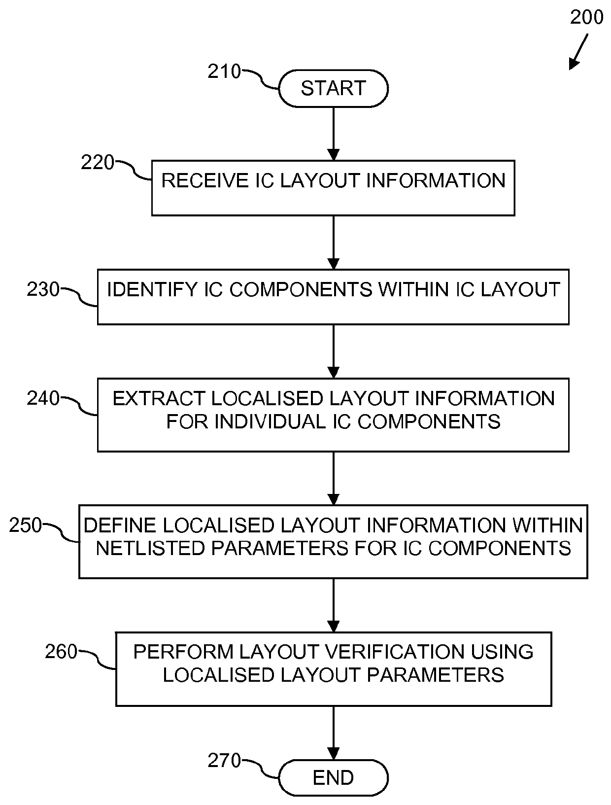
[0018]Referring first to FIG. 1, there is illustrated a simplified block diagram of an example of an apparatus 100 for performing verification of integrated circuit layouts. Because the illustrated embodiments of the present invention may for the most part, be implemented using electronic components and circuits known to those skilled in the art, details will not be explained in any greater extent than that considered necessary as illustrated below, for the understanding and appreciation of the underlying concepts of the present invention and in order not to obfuscate or distract from the teachings of the present invention.

[0019]In the illustrated example, the apparatus 100 comprises at least one signal processing module 110 arranged to perform the verification of integrated circuit layouts. For example, the signal processing module(s) 110 may be arranged to execute computer-readable code stored within one or more non-transitory computer program products, such as illustrated general...


PUM


Abstract

A method of performing layout verification for an integrated circuit (IC) layout is described. The method comprises receiving layout information for the IC layout, identifying at least one IC component within the IC layout, extracting localized layout information for the at least one IC component from the received layout information, defining the localized layout information for the at least one IC component within at least one component instance parameter therefor, and performing at least one layout verification check for the at least one component based at least partly on the at least one component instance parameter.

Description

FIELD OF THE INVENTION[0001]This invention relates to a method and apparatus for performing integrated circuit layout verification.BACKGROUND OF THE INVENTION[0002]Physical verification is the process of checking, using electronic design automation (EDA) software tools, whether an integrated circuit (IC) layout design meets certain criteria. IC layout is the representation of the IC in terms of planar geometric shapes which correspond to the patterns of metal, oxide and / or semiconductor layers that make up the components of the integrated circuit. Within the physical verification process, a layout generated for an IC is typically required to pass a series of checks. Such checks typically include design rule checking (DRC), layout versus schematic (LVS) checks, etc.[0003]DRC is used to determine whether the physical layout of a particular IC layout satisfies a series of recommended parameters called design rules. The design rules are a series of parameters provided by a semiconductor...

Claims


Application Information

Patent Timeline
Patent Type & Authority Patents(United States)
IPC IPC(8): G06F17/50H01L21/027
CPCG06F17/5081H01L21/027Y02T10/82G06F30/398
Inventor HOURS, XAVIERARORA, SHITIZRUTH, ROBERT SCOTT
Owner NXP USA INC