Development of high etch selective hardmask material by ion implantation into amorphous carbon films

a technology of amorphous carbon film and high etch selective hardmask, which is applied in the direction of semiconductor/solid-state device manufacturing, basic electric elements, electric apparatus, etc., can solve the problems of increasing compressive stress, increasing the hardness of the hardmask, and reducing the application range of the hardmask, so as to improve the patterning effect, increase the hardness and density of the hardmask, and maintain or reduce the internal stress of the hardmask

Active Publication Date: 2016-08-09
APPLIED MATERIALS INC
View PDF9 Cites 23 Cited by
  • Summary
  • Abstract
  • Description
  • Claims
  • Application Information

AI Technical Summary

Benefits of technology

[0009]Embodiments described herein provide for a method of forming an etch selective hardmask. An amorphous carbon hardmask is implanted with various dopants to increase the hardness and density of the hardmask. The ion implantation of the amorphous carbon hardmask also maintains or reduces the internal stress of the hardmask. The etch selective hardmask generally provides for improved patterning in advanced NAND and DRAM devices.

Problems solved by technology

A lower compressive stress eliminates undesirable wafer bow after hardmask deposition, which can make further device fabrication difficult.
Current hardmasks are insufficient for developing next generation NAND and DRAM devices.
However, current attempts at increasing etch selectivity have resulted in an increase in compressive stress, and attempts at decreasing compressive stress have resulted in a decrease in etch selectivity.

Method used


Image

  • Development of high etch selective hardmask material by ion implantation into amorphous carbon films
  • Development of high etch selective hardmask material by ion implantation into amorphous carbon films
  • Development of high etch selective hardmask material by ion implantation into amorphous carbon films

Examples


Embodiment Construction

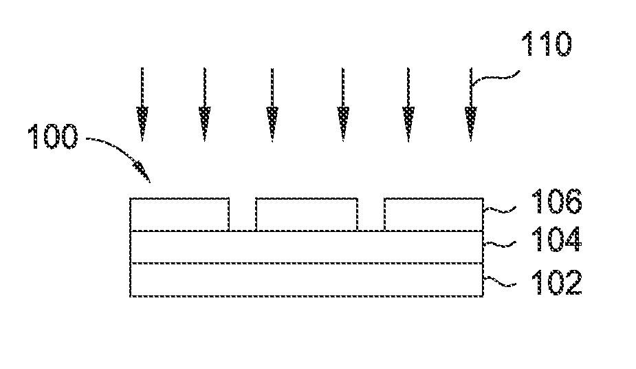
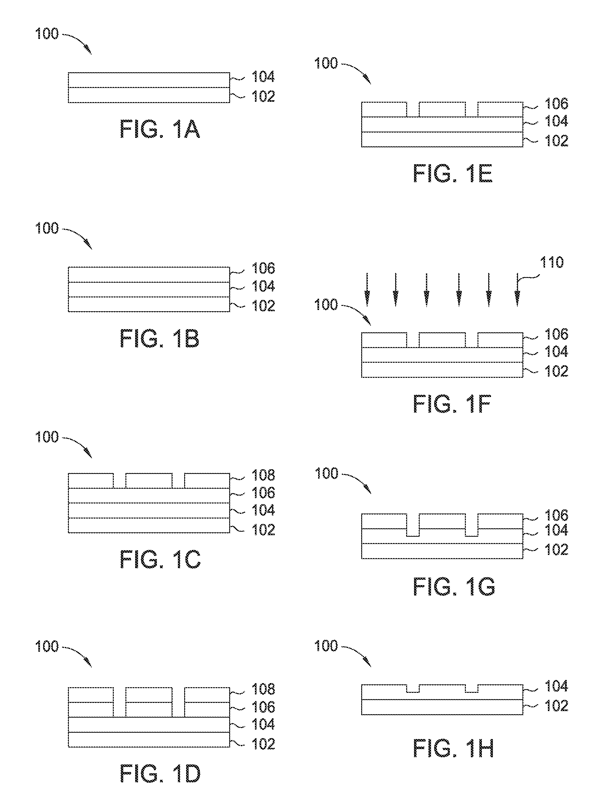
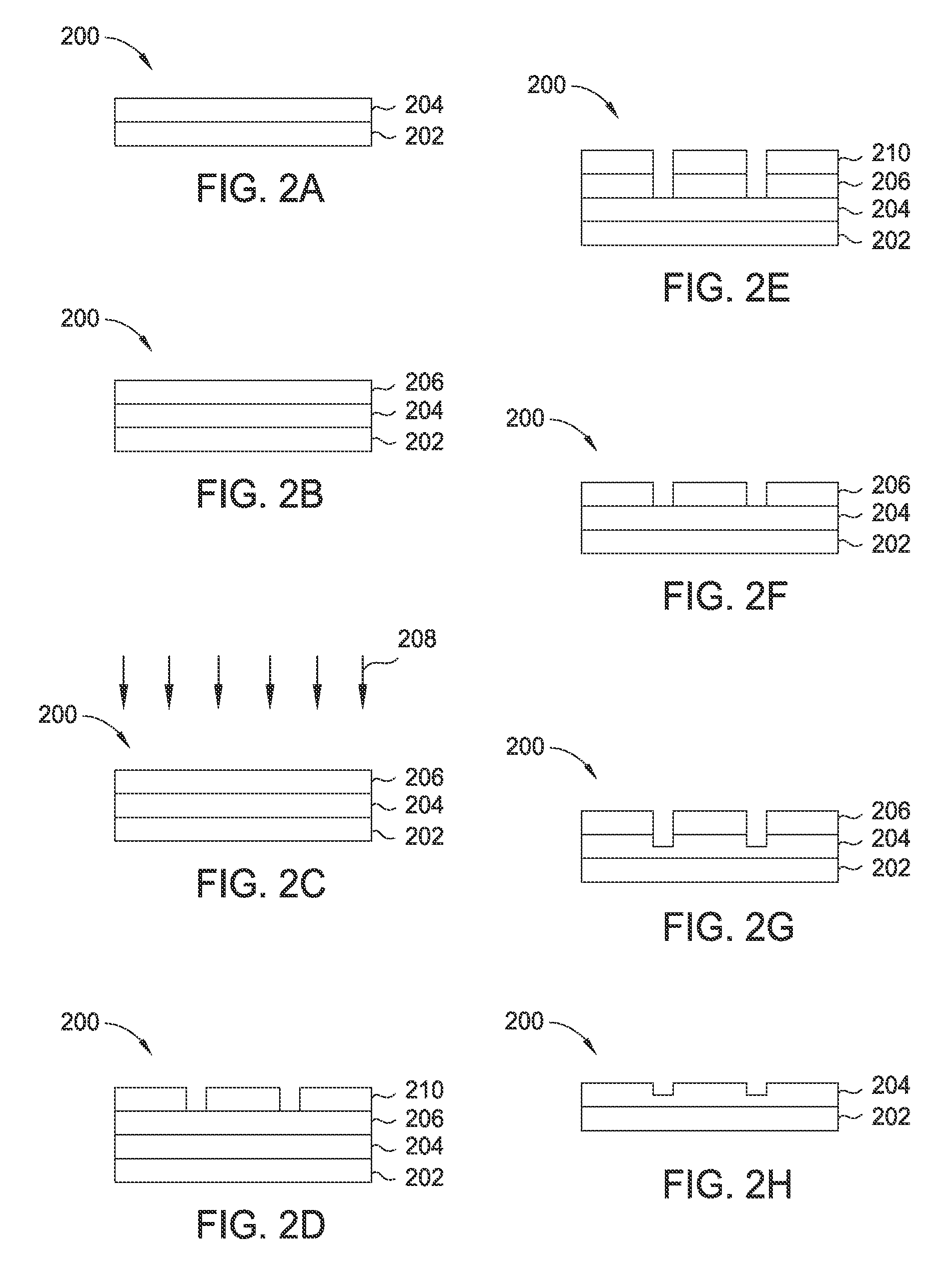
[0017]Ideal hardmask materials should exhibit very high etch resistance when compared to the etching of underlayer materials, such as dielectric stacks. In addition the hardmask materials should also exhibit low stress and strong mechanical properties. Lower stress generally reduces or eliminates undesirable wafer bow after hardmask deposition whereas increased hardness generally reduces undesirable line bending of high aspect ratio structures after the hardmask is opened.

[0018]Embodiments described herein provide for a method of forming an etch selective hardmask. An amorphous carbon hardmask is implanted with various dopants to increase the hardness and density of the hardmask. The ion implantation of the amorphous carbon hardmask also maintains or reduces the internal stress of the hardmask. The etch selective hardmask generally provides for improved patterning in advanced NAND and DRAM devices.

[0019]FIGS. 1A-1H are schematic, cross-sectional views of a stack 100 illustrating a h...


PUM

PropertyMeasurementUnit
thicknessaaaaaaaaaa
thicknessaaaaaaaaaa
thicknessaaaaaaaaaa

Abstract

Embodiments described herein provide for a method of forming an etch selective hardmask. An amorphous carbon hardmask is implanted with various dopants to increase the hardness and density of the hardmask. The ion implantation of the amorphous carbon hardmask also maintains or reduces the internal stress of the hardmask. The etch selective hardmask generally provides for improved patterning in advanced NAND and DRAM devices.

Description

CROSS-REFERENCE TO RELATED APPLICATIONS[0001]This application claims benefit of U.S. Provisional Patent Application Ser. No. 61 / 925,139, filed Jan. 8, 2014, which is incorporated herein by reference.BACKGROUND[0002]1. Field[0003]Embodiments described herein generally relate to methods of forming hardmask materials for semiconductor devices. More specifically, embodiments described herein relate to the development of a high etch selective hardmask material by ion implantation into amorphous carbon films.[0004]2. Description of the Related Art[0005]Hardmasks are used to fabricate NAND and dynamic random access memory (DRAM) devices. Hardmasks are commonly used as sacrificial layers in lithographic patterning and enable, through an etching process, the patterning of features onto a layer of a semiconductor device. The patterned features can form, for example, the transistors and interconnects that allow the NAND and DRAM devices to operate.[0006]The important properties of a hardmask m...

Claims


Application Information

Patent Timeline
Patent Type & Authority Patents(United States)
IPC IPC(8): H01L21/308H01L21/311H01L21/3115
CPCH01L21/3086H01L21/31144H01L21/31155H01L21/324
Inventor MANNA, PRAMITMALLICK, ABHIJIT BASUGODET, LUDOVICCHEN, YONGMEIXUE, JUNSRINIVASAN, MUKUNDYIEH, ELLIE Y.NEMANI, SRINIVAS D.
Owner APPLIED MATERIALS INC
Why Eureka
Try Eureka