Tactile array sensor

a technology of array sensor and actuator, applied in the field of multi-point sensing, can solve problems such as dielectric layer compression, and achieve the effects of reducing the need for expensive infrastructure, high resolution, and facilitating weaving fabri

Active Publication Date: 2016-08-16
NAIDU PRAKASH C R J
View PDF9 Cites 7 Cited by
  • Summary
  • Abstract
  • Description
  • Claims
  • Application Information

AI Technical Summary

Benefits of technology

[0010]According to an aspect of the disclosed invention, the conductors are insulated and thus can continue to longer lengths on both sides of the tactile array eliminating the need for a joint or connection interface near periphery of the sensor array. This also allows for the sensor data processing circuit such as an IC to be relatively further away from the sensor array, facilitating remotely centralized circuit that may be attached to several sensor arrays; particularly advantageous for robots wherein fingers and other robot parts may need separate sensor arrays.
[0011]According to another aspect of the disclosed invention, the conductors are insulated and hence can be placed very close to each other at micro-millimeter center to center distance resolution by simple manual, semi-automated, or fully automated methods without relatively expensive methods such as PVD, photolithography or soft lithography and eliminating the need for expensive infrastructure such as clean room environment.
[0012]Courting to an additional but optional aspect of the disclosed invention, in one of the embodiments, the insulation of the conductors themselves is used for realizing the capacitor pixels, eliminating the need for a separate dielectric layer between the conductor layers. Furthermore, additionally, but optionally, this embodiment of the disclosed invention allows use of stretchable conductors of micro and even nano diameter size such as transparent conductive Graphene nanoribbons with transparent, flexible and stretchable insulation such as PDMS coating that can facilitate woven fabric like sensor array with very high resolution and good stretchable characteristics in both warp and weft directions.
[0013]In yet another embodiment of the disclosed invention, reduction of the burden of number of connections at one layer of conductors in the sensor is achieved by having radial conductor electrodes wherein the conductors can be electrically connected conveniently to a common terminal at one end at the center of the sensor array. Furthermore, additionally, but optionally, an aspect of this embodiment of the disclosed invention is reduction of the overall computation burden of the sensor by having a broader resolution of sensor array at peripheral region while maintaining a closer resolution of sensing array at a central region of the sensor. This is particularly of importance in biomimetic robotic hands as living beings have differential sensing resolutions at different areas of sensing organs depending on salience of sensing needs.
[0014]In addition, and optionally, a further embodiment of the disclosed invention achieves reduction of the burden of number of connections at one layer of conductors in the sensor by having a layer with single spiral conductor with only one end of the spiral as terminal while having individual pixel electrodes in the other layer again in spiral configuration allowing distinct identification defining a location of a contact sensing.
[0015]In yet another embodiment of the disclosed invention, the sensing pad assemblies are modular in configuration allowing flexibility in deployment such as different resolution in different regions depending on regional requirements, and moreover a defective sensor pad does not result in requirement of an entire sensor array to be repaired or replaced as just an individual sensor pad can be separately replaced. Moreover, in this embodiment of the disclosed invention, a conductive surface with micro-holes allowing passage of insulated conductors connected to the sensor pads is used as a common ground, thus reducing wiring and connections associated with a layer of conduction.

Problems solved by technology

A contact on the surface of external layer causes pressure and resulting compression of the dielectric layer.

Method used


Image

  • Tactile array sensor
  • Tactile array sensor
  • Tactile array sensor

Examples


Embodiment Construction

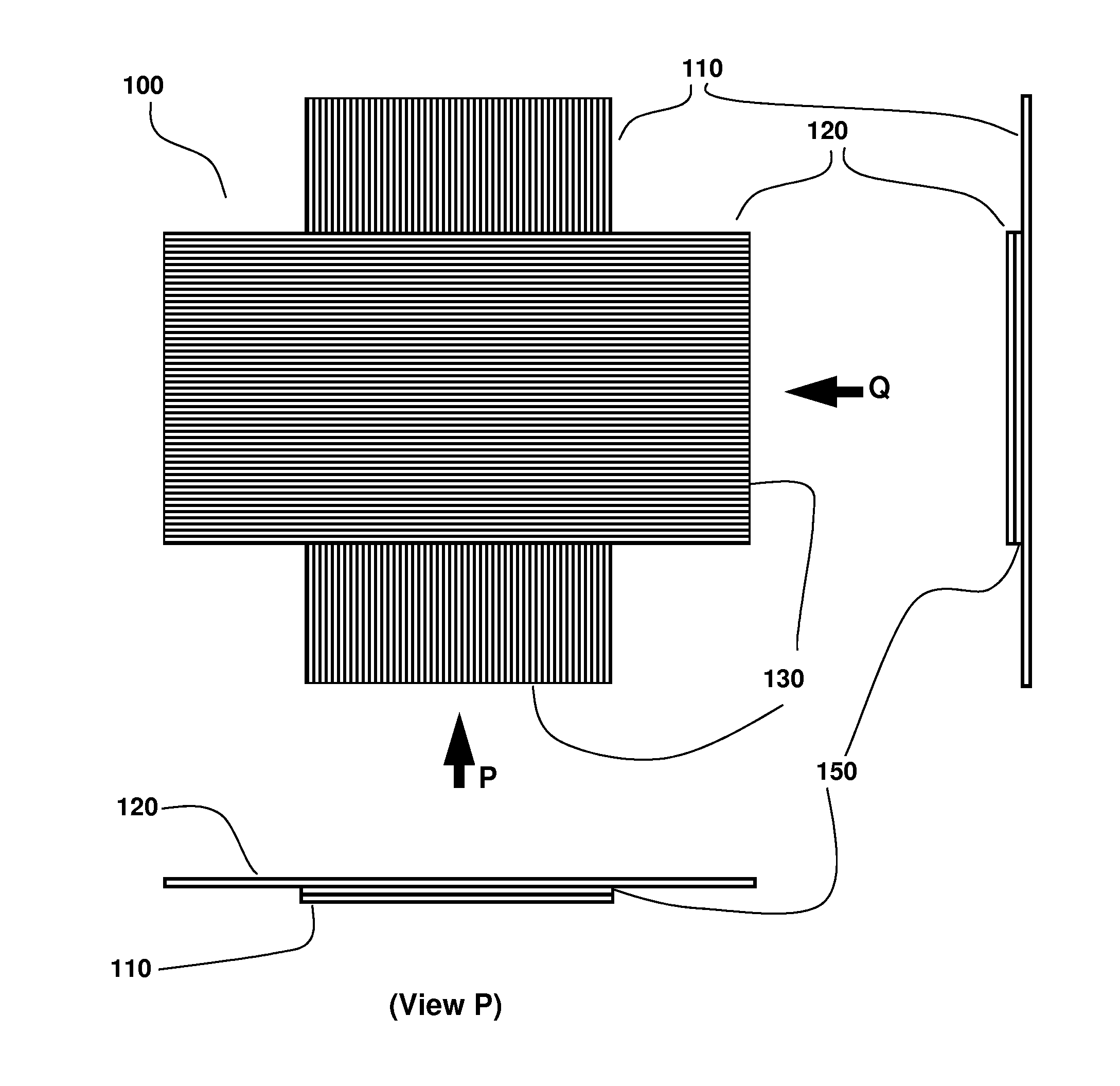
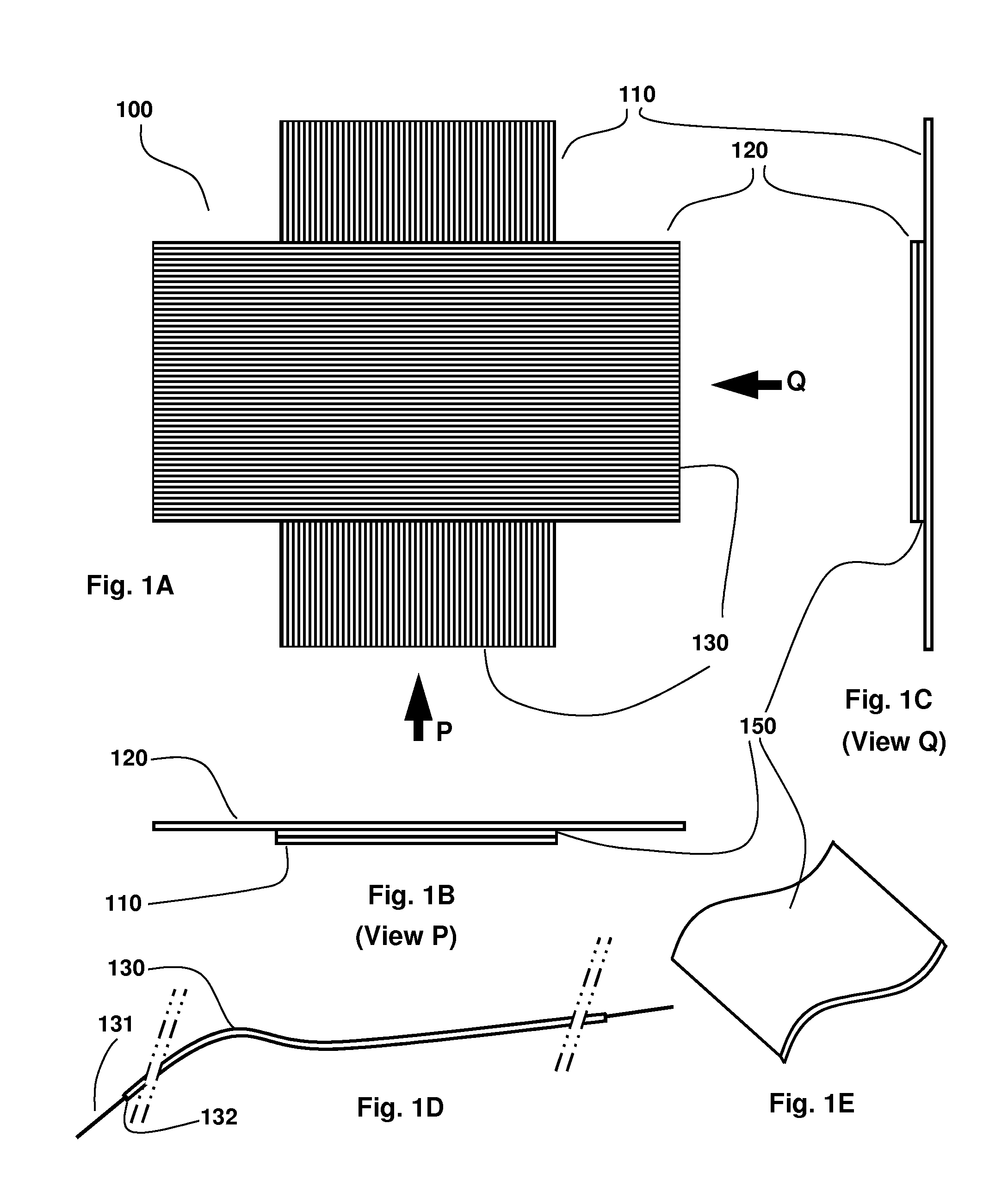
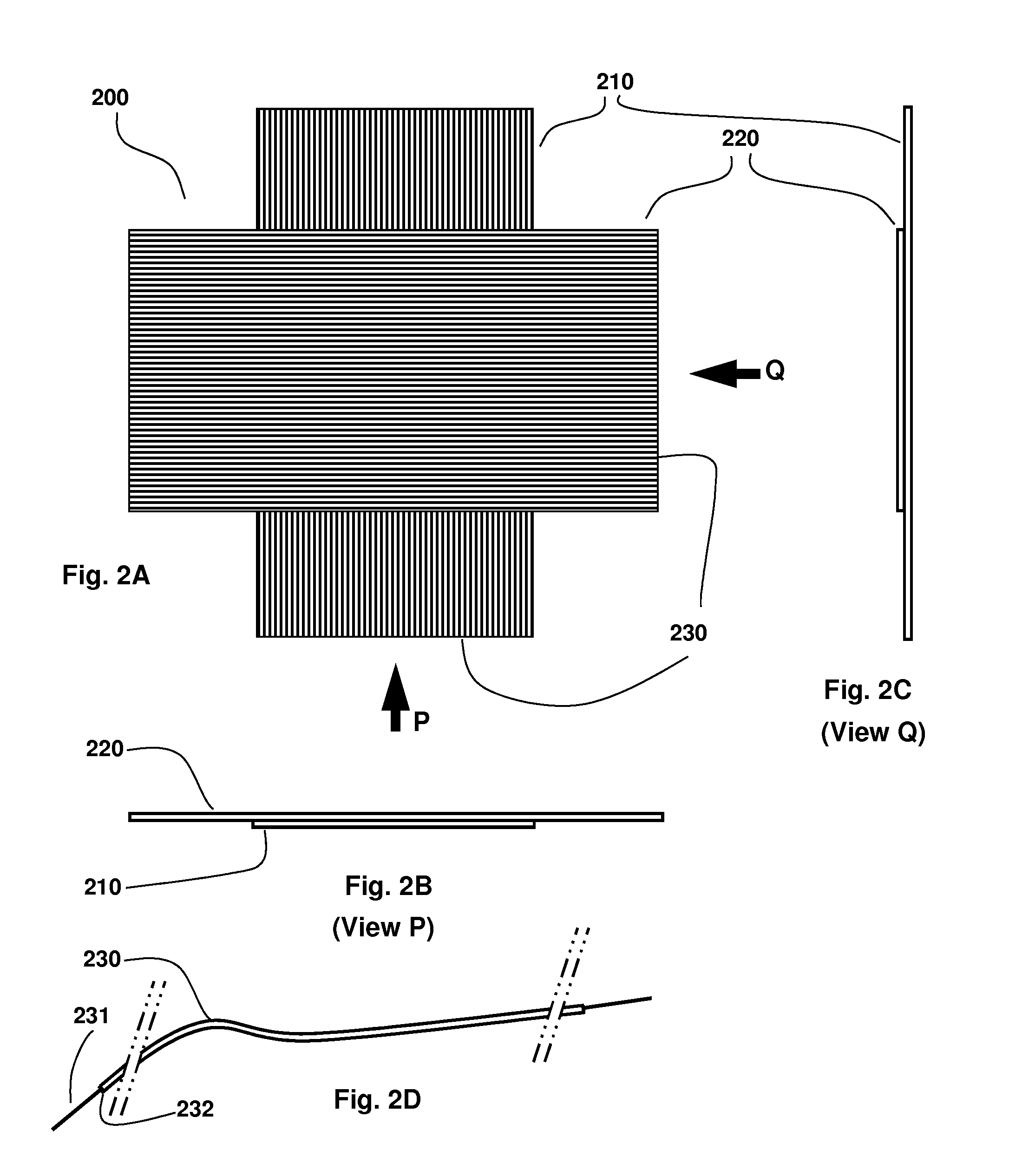
[0022]A first embodiment 100 of the disclosed invention is illustrated in FIG. 1A wherein one set of insulated conductor electrodes 130 are laid in one layer 110, another set of insulated conductor electrodes 130 are laid in another layer 120 at substantially orthogonal direction to the electrodes in the first layer; the insulated conductor electrode layers separated by a dielectric material layer 150 (shown in FIG. 1E). The end views P and Q illustrated in FIGS. 1B and 1C show the arrangement of these layers relative to each other. The intersections of insulated conductors sandwiching dielectric material in-between form capacitor pixels that function as an array of the tactile sensor. In one option of this embodiment, the dielectric material is Polydimethylsiloxane (PDMS). In a second option of this embodiment, the dielectric material is a tape or sheet made of a dielectric material with dielectric constant comparable to or greater than the dielectric constant of PDMS (2.3 to 2.8),...


PUM


Abstract

A capacitance based tactile array sensor is disclosed that provides for close resolution of sensing pixels by using insulated conductors as electrodes, and allows for eliminating the need for a joint or connection interface near periphery of the sensor array. Optional aspects of the invention include provision for allowing use of stretchable conductors, reduction of the burden of number of connections at one layer of conductors in the sensor, providing for differential sensing resolutions at different areas of sensing, and modularity in configuration allowing replacement of a defective sensor pixel in the array. The tactile array sensor may be integrated with surface of a robotic hand's finger, palm, or any other surface of a device that requires multi-point sensing of external contacts. The capacitance information is processed for useful display or control of systems based on the contact feedback.

Description

RELATED U.S. PROVISIONAL PATENT APPLICATION[0001]This application claims the benefit of U.S. Provisional Patent Application No. 61 / 705,137, filed 24 Sep. 2012, including all the written description of the inventions described therein and making claim to the inventions disclosed therein.STATEMENT REGARDING FEDERALLY SPONSORED RESEARCH OR DEVELOPMENT[0002]The work on which the disclosure of this application is based is partially funded by National Science Foundation (NSF) under the Small Business Innovation Research (SBIR) program.BACKGROUND OF THE INVENTION[0003]This invention relates to multi-point sensing of a contact with an external surface of a device. The device may be a robot hand, a robot body part, or any other component or part of any system that requires sensing an external contact with another body or part in the proximity environment with certain preferred parameters. For example, in order to be as similar to human skin as possible, robot skin needs to be flexible to ena...

Claims


Application Information

Patent Timeline
Patent Type & Authority Patents(United States)
IPC IPC(8): G01R27/26B25J9/16H03K17/96G06F1/00
CPCH03K17/962B25J9/1694G01R27/2605H03K2017/9602G05B2219/40625G09G2230/00G06F2101/00G06F1/00
Inventor NAIDU, PRAKASH C R JMANDAYAM, SRINIVASAN ANAIDU, KSHIRSAGAR C J
Owner NAIDU PRAKASH C R J
Why Eureka
Try Eureka