Flip-chip LED and fabrication method thereof

a technology of flip-chip led and fabrication method, which is applied in the direction of basic electric elements, electrical apparatus, and semiconductor devices, can solve the problems of reduced light extraction efficiency, limited material thickness, and low concentration of hole carriers, and achieve the effect of improving the light extraction efficiency of led

Inactive Publication Date: 2016-08-16
ENRAYTEK OPTOELECTRONICS
View PDF12 Cites 0 Cited by
  • Summary
  • Abstract
  • Description
  • Claims
  • Application Information

AI Technical Summary

Benefits of technology

[0006]It is an aim of the present invention to provide a method that can improve the light extraction efficiency of a flip-chip LED.
[0027]As described above, in the method according to the present invention, a first metal layer is formed on a p-type GaN layer and annealed for self-assembly and then serves as a mask in an etching process carried out on the p-type GaN layer. Afterward, a second metal layer is deposited, which, together with the first metal layer, forms an uneven metal reflector layer. At this layer, light emitted from the active layer is scattered and finally exits rather than being confined in a wave guiding structure formed by the layers of the LED. This results in an improvement in the light extraction efficiency of the LED.

Problems solved by technology

In the fabrication of a conventional LED, there is a difficulty in p-type doping of gallium nitride (GaN) material, which leads to a low concentration of hole carriers and limitations to the thickness of the material and thus forms a barrier for current diffusion.
However, use of the current spreading layer is also associated with some issues.
On the one hand, the current spreading layer partially absorbs light and causes a reduction in light extraction efficiency.
On the other hand, thinning the current spreading layer will make it less effective to form uniform and reliable current spread over the p-type GaN material.
Therefore, its use requires a proper compromise between the light extraction efficiency and the current spread effect.
This will inevitably impose limitations on further improvement of its power conversion efficiency.
In addition, in the conventional LED, as electrodes and leads are arranged on the same side of a light-generating region, light is partially blocked away during operation and the efficiency of the conventional LED is thus limited.
Further, the conventional LED relies on a sapphire substrate with a very low thermal conductivity for dissipation of heat from its p-n junction.
This will lead to a very long heat conduction path in case of a power LED device having a large size.
As a result, the conventional LED will have high thermal impedance, as well as a limited operating current.
However, this architecture makes part of the light confined in a wave guiding structure formed by the layers of the LED.
This is detrimental to the light extraction efficiency.

Method used


Image

  • Flip-chip LED and fabrication method thereof
  • Flip-chip LED and fabrication method thereof
  • Flip-chip LED and fabrication method thereof

Examples


Embodiment Construction

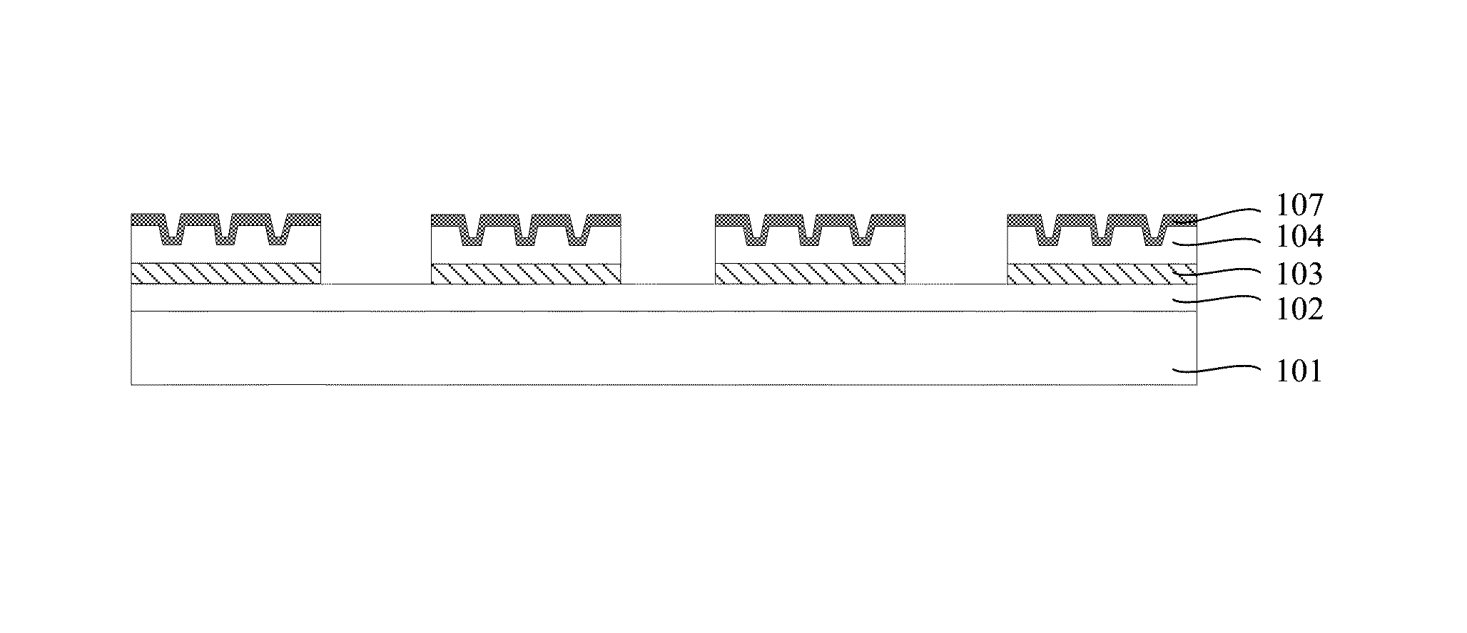
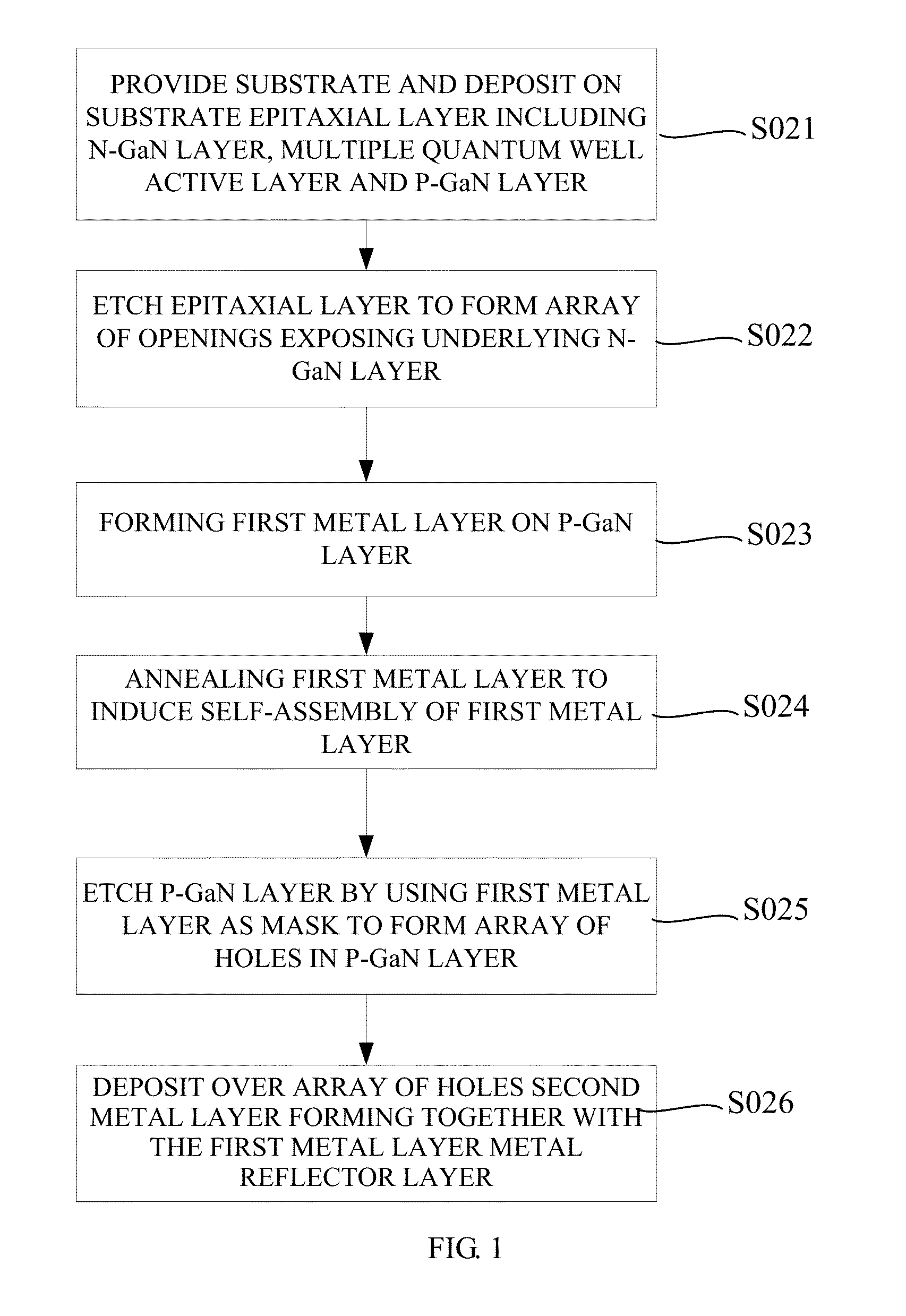
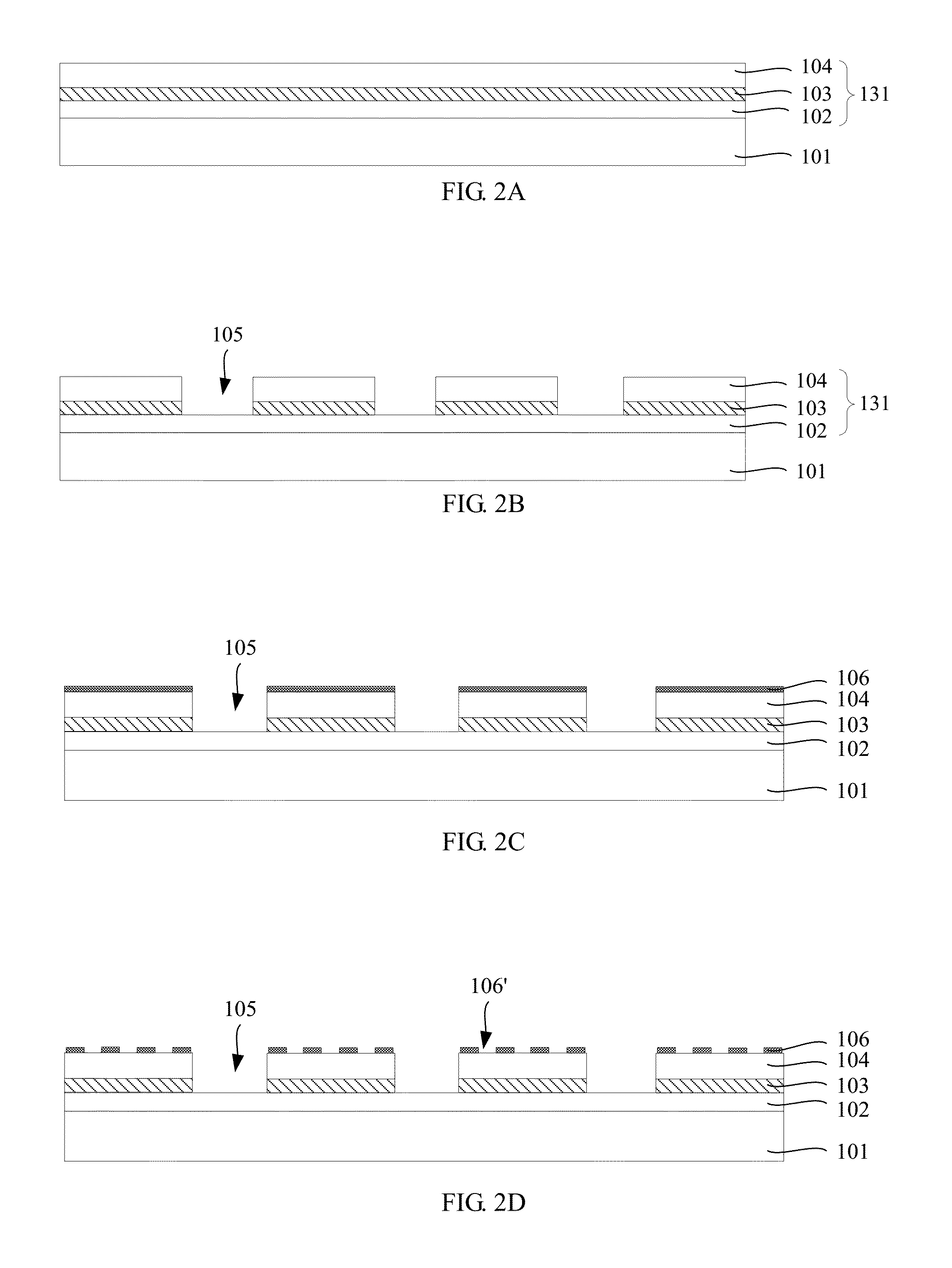
[0030]As has been mentioned in the Background section, the existing metal reflector layer still has impact on the light extraction efficiency of the flip-chip LED. The present invention provides a flip-chip LED and a fabrication method thereof. In the fabrication method of the flip-chip LED, a first metal layer is formed and annealed for self-assembly and then a p-type GaN layer is etched by using the first metal layer as a mask. Afterward, a second metal layer is deposited, which, together with the first metal layer, forms an uneven metal reflector layer which results in an improved light extraction efficiency of the flip-chip LED.

[0031]The present invention will be described in greater detail in the following description demonstrating preferred embodiments of the invention, which are to be read in conjunction with the accompanying drawings. Those of skill in the art should, in light of the present disclosure, appreciate that many changes can be made in the specific embodiments dis...


PUM

PropertyMeasurementUnit
thicknessaaaaaaaaaa
temperatureaaaaaaaaaa
thicknessaaaaaaaaaa

Abstract

A flip-chip LED and a method for forming the LED are disclosed. The method includes: providing a substrate and depositing on the substrate an epitaxial layer including, from the bottom upward, an n-type GaN layer, a multi-quantum well active layer, and a p-type GaN layer; etching the epitaxial layer to form an array of openings exposing the n-type GaN layer; forming a first metal layer on the p-type GaN layer; annealing the first metal layer to induce self-assembly thereof; etching the p-type GaN layer by using the first metal layer as a mask such that an array of holes formed therein; and depositing a second metal layer over the array of holes, the second metal layer and the first metal layer form a metal reflector layer. The design can result in an improvement in the light extraction efficiency of the LED.

Description

TECHNICAL FIELD[0001]The present invention relates to the fabrication of light-emitting diodes (LEDs) and, more particularly, to a flip-chip LED and a fabrication method thereof.BACKGROUND[0002]In the fabrication of a conventional LED, there is a difficulty in p-type doping of gallium nitride (GaN) material, which leads to a low concentration of hole carriers and limitations to the thickness of the material and thus forms a barrier for current diffusion. In order to obtain uniform current distribution, a current spreading layer is typically formed over the p-type GaN material.[0003]However, use of the current spreading layer is also associated with some issues. On the one hand, the current spreading layer partially absorbs light and causes a reduction in light extraction efficiency. On the other hand, thinning the current spreading layer will make it less effective to form uniform and reliable current spread over the p-type GaN material. Therefore, its use requires a proper compromi...

Claims


Application Information

Patent Timeline
Patent Type & Authority Patents(United States)
IPC IPC(8): H01L33/00H01L33/40H01L33/06H01L33/60H01L33/38H01L33/20
CPCH01L33/007H01L33/382H01L33/06H01L33/60H01L33/40H01L33/0079H01L33/0095H01L33/20H01L2933/0016H01L33/405H01L2933/0058H01L33/0093H01L2224/14H01L2224/16225
Inventor YU, HONGBO
Owner ENRAYTEK OPTOELECTRONICS
Why Eureka
Try Eureka