Semiconductor element including active region, low resistance layer and vertical drift portion

a technology of active region and low resistance layer, applied in the field of semiconductor devices, can solve the problems of increasing breakdown voltage, increasing loss, and device being destroyed by thermal runaway, and achieves the effects of reducing the amount of carriers accumulated, reducing the concentration of current, and increasing the reverse recovery capability (breakdown withstand)

Active Publication Date: 2016-09-06
FUJI ELECTRIC CO LTD
View PDF14 Cites 5 Cited by
  • Summary
  • Abstract
  • Description
  • Claims
  • Application Information

AI Technical Summary

Benefits of technology

[0015]The invention, in order to resolve the problems of the heretofore described existing technology, has an object of providing a semiconductor device such that it is possible to increase breakdown withstand, using a superjunction semiconductor device wherein it is possible to considerably improve the trade-off relationship between on-state resistance and breakdown voltage.
[0023]According to the invention, the volume of an n+ type drain layer (the first conductivity type low resistance layer) in an edge termination region is reduced by a p+ type drain region (the second conductivity type low resistance layer) being selectively provided inside the n+ type drain layer in the edge termination region, because of which the injection of electrons from the n+ type drain layer on the substrate back surface side into a second parallel p-n structure is suppressed, together with which the injection of holes from an outermost p-type base region on the substrate front surface side into the second parallel p-n structure is suppressed. Because of this, it is possible to reduce the amount of carriers accumulated in the edge termination region, and thus possible to alleviate the concentration of current flowing into the outermost p-type base region during a parasitic diode reverse recovery process. Consequently, it is possible to increase reverse recovery capability (breakdown withstand).
[0024]According to the semiconductor device according to the invention, an advantage is achieved in that it is possible to increase breakdown withstand.

Problems solved by technology

Meanwhile, a portion of the high-resistance n− type drift layer depletes when in an off-state, increasing breakdown voltage.
Conversely, a semiconductor device with high breakdown voltage is such that the n− type drift layer is thick, because of which the on-state resistance increases, and loss increases.
Also, there is a problem in that when the leakage current in an off-state increases too far, the device is destroyed by thermal runaway.

Method used


Image

  • Semiconductor element including active region, low resistance layer and vertical drift portion
  • Semiconductor element including active region, low resistance layer and vertical drift portion
  • Semiconductor element including active region, low resistance layer and vertical drift portion

Examples


embodiment 1

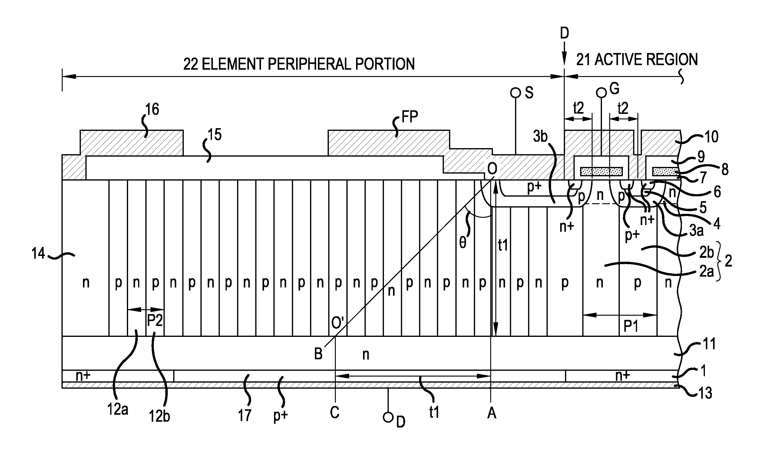
[0031]A description will be given of the structure of a semiconductor device according to Embodiment 1, using an n-channel vertical MOSFET with a planar gate structure as an example. FIG. 1 is a sectional view showing the structure of the semiconductor device according to Embodiment 1. The semiconductor device according to Embodiment 1 shown in FIG. 1 is a superjunction MOSFET including a drain drift portion (vertical drift portion) 2 of a first parallel p-n structure. A p-type base region 3a with a high impurity concentration, which forms an active region 21, is selectively provided in a surface layer on one surface side (hereafter taken to be a substrate front surface side) of the drain drift portion 2. The substrate is an epitaxial substrate, to be described hereafter.

[0032]A p+ type contact region 5 and n+ type source region 6 with high impurity concentrations are selectively provided on the substrate front surface side inside the p-type base region 3a. The n+ type source region...

embodiment 2

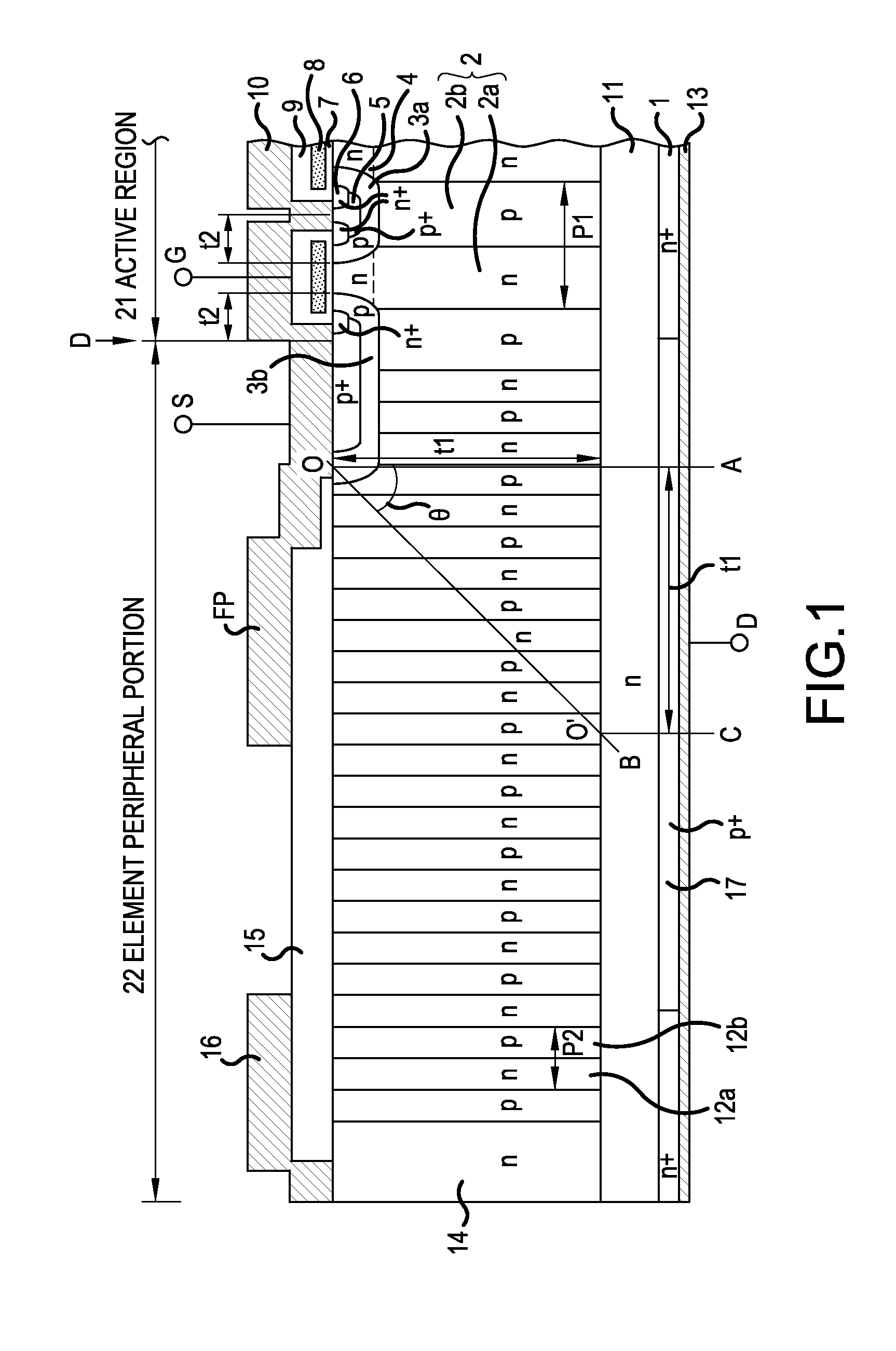
[0056]A description will be given of the structure of a superjunction semiconductor device according to Embodiment 2. FIG. 2 is a sectional view showing the structure of the semiconductor device according to Embodiment 2. The superjunction semiconductor device according to Embodiment 2 differs from the superjunction semiconductor device according to Embodiment 1 in that an n-type bulk region 31 contiguous with a first parallel p-n structure is provided in place of a second parallel p-n structure, and a p-type RESURF region 32 is provided in a surface layer on the substrate front surface side of the n-type bulk region 31.

[0057]The n-type bulk region 31 is a region between a first parallel p-n structure provided from the active region 21 to the edge termination region 22 and the n-type channel stopper region 14 provided farthest to the exterior in the edge termination region 22. The p-type RESURF region 32 is selectively provided in a surface layer on the substrate front surface side ...

embodiment 3

[0060]A description will be given of the structure of a superjunction semiconductor device according to Embodiment 3. FIG. 3 is a sectional view showing the structure of the semiconductor device according to Embodiment 3. The superjunction semiconductor device according to Embodiment 3 differs from the superjunction semiconductor device according to Embodiment 1 in that an outer end portion of a p+ type drain region 41 is extended as far as the outer periphery (a substrate side surface) of the edge termination region 22. Configurations other than this of the superjunction semiconductor device according to Embodiment 3 are the same as those of the superjunction semiconductor device according to Embodiment 1. The method of manufacturing the superjunction MOSFET according to Embodiment 3 is the same as the method of manufacturing the superjunction semiconductor device according to Embodiment 1, except that the formation range of the p+ type drain region 41 differs.

[0061]As heretofore d...


PUM


Abstract

A drain drift portion is a first parallel p-n structure, largely corresponding to a portion directly below a p-type base region forming an active region, formed by first n-type regions and first p-type regions being alternately and repeatedly joined. The periphery of the drain drift portion is an edge termination region formed of a second parallel p-n structure aligned contiguously to the first parallel p-n structure and formed by second n-type regions and second p-type regions being alternately and repeatedly joined. An n-type buffer layer is provided between the first and second parallel p-n structures and an n+ type drain layer. A p+ type drain region is selectively provided inside the n+ type drain layer in the edge termination region, penetrating the n+ type drain layer in the depth direction.

Description

CROSS-REFERENCE TO RELATED APPLICATIONS[0001]This application is a continuation of International Application No. PCT / JP 2013 / 082747, filed on Dec. 5, 2013, which is based on and claims priority to Japanese Patent Application No. JP 2013-005811, filed on Jan. 16, 2013. The disclosure of the Japanese priority application and the PCT application in their entirety, including the drawings, claims, and the specification thereof, are incorporated herein by reference.BACKGROUND OF THE INVENTION[0002]1. Field of the Invention[0003]The present invention relates to a semiconductor device.[0004]2. Related Art[0005]Generally, semiconductor devices are categorized into lateral semiconductor devices, which have an electrode on one surface, and vertical semiconductor devices, which have an electrode on both surfaces. Vertical semiconductor devices are such that the direction in which a drift current flows when in an on-state and the direction in which a depletion layer caused by reverse bias voltag...

Claims


Application Information

Patent Timeline
Patent Type & Authority Patents(United States)
IPC IPC(8): H01L29/06H01L29/78H01L29/10H01L29/40H01L21/263H01L21/265
CPCH01L29/7811H01L29/063H01L29/0634H01L29/1095H01L21/263H01L21/26506H01L29/0638H01L29/402
Inventor ONISHI, YASUHIKO
Owner FUJI ELECTRIC CO LTD
Why Eureka
Try Eureka