Elastic wave device, high-frequency front end circuit, and communication apparatus

a technology of elastic wave and front end circuit, which is applied in the direction of chemistry apparatus and processes, polycrystalline material growth, crystal growth process, etc., can solve the problems of fractional bandwidth increase, deterioration of frequency temperature characteristic, and increase of fractional bandwidth, so as to improve the trade-off relationship between frequency temperature characteristic and fractional bandwidth and reduce the electrical resistance of the idt electrode

Active Publication Date: 2022-06-21
MURATA MFG CO LTD
View PDF5 Cites 2 Cited by
  • Summary
  • Abstract
  • Description
  • Claims
  • Application Information

AI Technical Summary

Benefits of technology

[0006]Preferred embodiments of the present invention provide elastic wave devices, high-frequency front end circuits, and communication apparatuses that are capable of improving a trade-off relationship between a frequency temperature characteristic and a fractional bandwidth while lowering an electrical resistance of an IDT electrode.
[0009]In this case, a fractional bandwidth is able to be effectively and stably increased. Therefore, a trade-off relationship between a frequency temperature characteristic and the fractional bandwidth can be further improved.
[0010]In an elastic wave device according to another preferred embodiment of the present invention, the first electrode layer includes Mo as the main component, and when a wave length which is defined by an electrode finger pitch of the IDT electrode is λ and a film thickness of the first electrode layer, which is normalized by the wave length λ, is hMo / λ(%), the film thickness hMo / λ of the first electrode layer is equal to or lower than about 30%. In this case, an increase in a stress of the first electrode layer is able to be reduced or prevented and the piezoelectric substrate will not be easily damaged.
[0019]In this case, the fractional bandwidth is able to be effectively and stably increased. Therefore, a trade-off relationship between the frequency temperature characteristic and the fractional bandwidth is able to be further improved.
[0020]In an elastic wave device according to another preferred embodiment of the present invention, the first electrode layer includes W as the main component, and when a wave length which is defined by an electrode finger pitch of the IDT electrode is λ and a film thickness of the first electrode layer, which is normalized by the wave length λ, is hW / λ(%), the film thickness hW / λ of the first electrode layer is equal to or lower than about 30%. In this case, an increase in a stress of the first electrode layer is able to be reduced or prevented and the piezoelectric substrate will not be easily damaged.
[0028]In an elastic wave device according to another preferred embodiment of the present invention, when a wave length which is defined by an electrode finger pitch of the IDT electrode is λ and a film thickness of the second electrode layer, which is normalized by the wave length λ, is hCu / λ(%), the film thickness hCu / λ of the second electrode layer is equal to or lower than about 15%. In this case, productivity is able to be improved.

Problems solved by technology

On the other hand, when the film thickness of the dielectric film made of silicon oxide is decreased, the fractional bandwidth is increased but the frequency temperature characteristic is deteriorated.
However, the inventors of the present invention have discovered that there is a problem of deterioration in the trade-off relationship between the frequency temperature characteristic and the fractional bandwidth because, as the film thickness of the Al layer is increased, the frequency temperature characteristic is deteriorated and the fractional bandwidth is not increased substantially.

Method used


Image

  • Elastic wave device, high-frequency front end circuit, and communication apparatus
  • Elastic wave device, high-frequency front end circuit, and communication apparatus
  • Elastic wave device, high-frequency front end circuit, and communication apparatus

Examples


Embodiment Construction

[0080]Hereinafter, the present invention will be explained by describing specific preferred embodiments of the present invention with reference to the drawings.

[0081]It should be noted that respective preferred embodiments which are described in the specification are exemplary and partial replacement or combination of components between different preferred embodiments may be made.

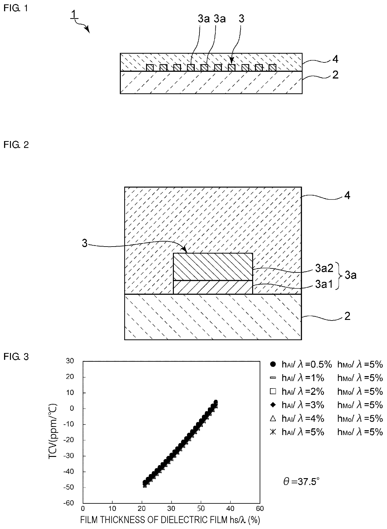
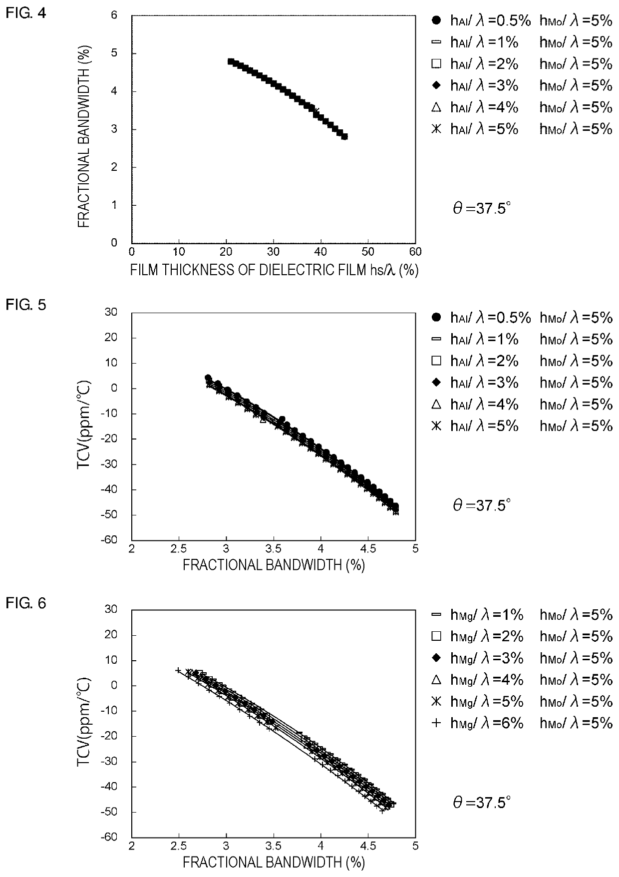
[0082]FIG. 1 is a cross-sectional front view of an elastic wave device according to a first preferred embodiment of the present invention. FIG. 2 is an enlarged cross-sectional front view of an electrode finger of an IDT electrode in the first preferred embodiment.

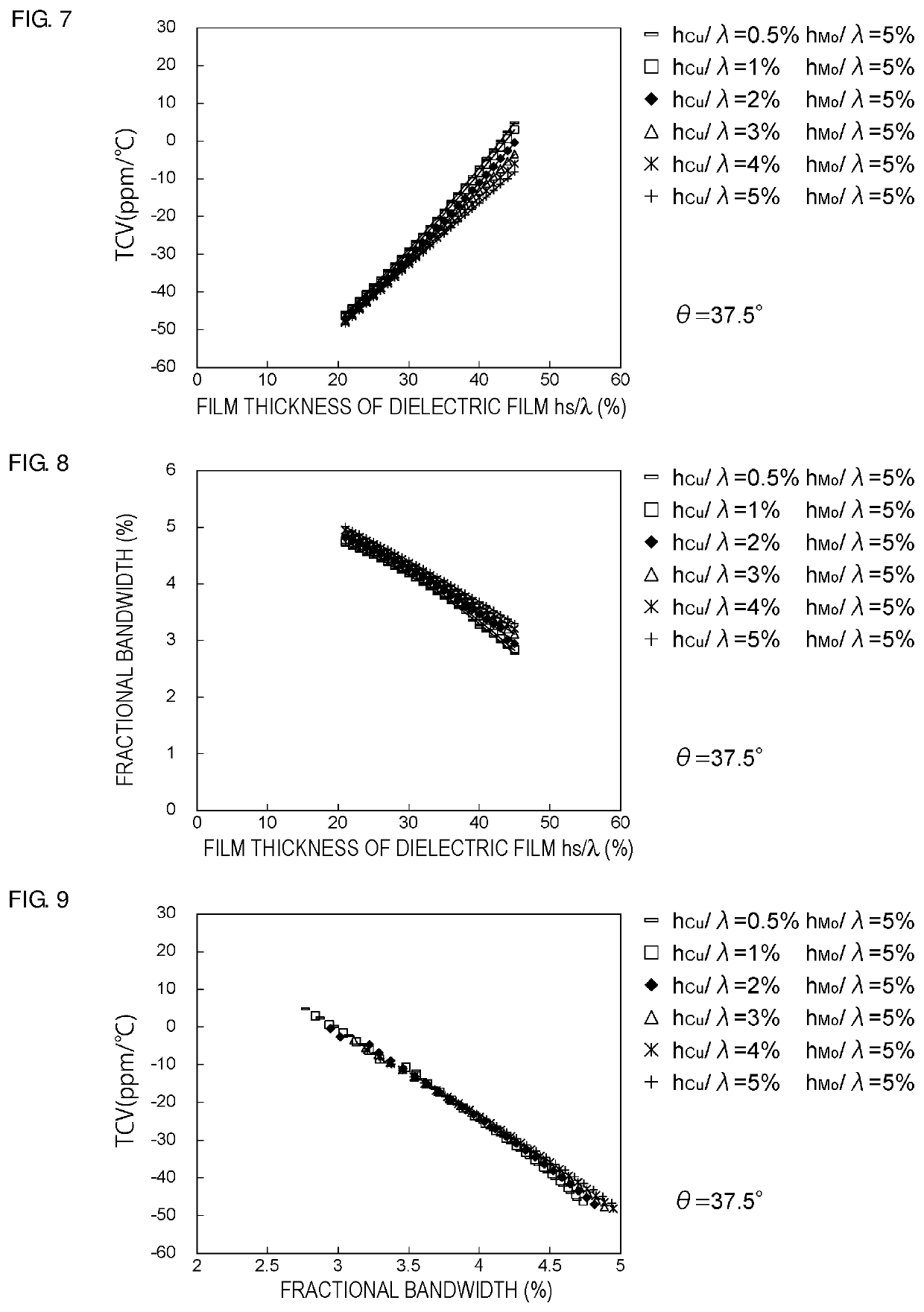
[0083]An elastic wave device 1 illustrated in FIG. 1 preferably utilizes Rayleigh waves. The elastic wave device 1 includes a piezoelectric substrate 2 preferably made of lithium niobate, for example. In the present preferred embodiment, Euler Angles (ϕ, θ, ψ) of the piezoelectric substrate 2 are preferably Euler Angles (0°, 37.5°, 0°), for exampl...


PUM

PropertyMeasurementUnit
Euler Anglesaaaaaaaaaa

Abstract

An elastic wave device includes a piezoelectric substrate, an IDT electrode including a first electrode layer located on the piezoelectric substrate and including one of Mo and W as a main component and a second electrode layer laminated on the first electrode layer and including Cu as a main component, and a dielectric film located on the piezoelectric substrate and covering the IDT electrode. The piezoelectric substrate is made of lithium niobate. The dielectric film is made of silicon oxide. The elastic wave device utilizes Rayleigh waves propagating along the piezoelectric substrate.

Description

CROSS REFERENCE TO RELATED APPLICATIONS[0001]This application claims the benefit of priority to Japanese Patent Application No. 2016-245758 filed on Dec. 19, 2016. The entire contents of this application are hereby incorporated herein by reference.BACKGROUND OF THE INVENTION1. Field of the Invention[0002]The present invention relates to an elastic wave device, a high-frequency front end circuit, and a communication apparatus.2. Description of the Related Art[0003]An existing elastic wave device has been widely used for a filter of a cellular phone or the like. International Publication No. 2011 / 158445, which will be described below, discloses an example of the elastic wave device. The elastic wave device includes a piezoelectric substrate made of LiNbO3. An IDT (interdigital transducer) electrode is provided on the piezoelectric substrate. The IDT electrode includes a multilayer metal film formed by laminating a Mo layer and an Al layer in this order from the piezoelectric substrate...

Claims


Application Information

Patent Timeline
Patent Type & Authority Patents(United States)
IPC IPC(8): H03H9/02H01L41/187H01L41/277H03H9/25H01L41/08H01L41/253C30B29/30H03H9/145
CPCH01L41/277C30B29/30H01L41/081H01L41/1873H01L41/253H03H9/02559H03H9/02574H03H9/02834H03H9/14541H03H9/25H10N30/057H10N30/04H10N30/8542H10N30/10513
Inventor SAJI, MARI
Owner MURATA MFG CO LTD
Why Eureka
Try Eureka