
Embedded touch screen liquid crystal display device and touch drive method thereof

a liquid crystal display device and touch drive technology, applied in the field of liquid crystal displays, can solve the problems of increasing the thickness of the touch panel lcd device, complex display system, and complex manufacturing process

Active Publication Date: 2016-09-13
SHANGHAI TIANMA MICRO ELECTRONICS CO LTD
View PDF28 Cites 35 Cited by
  • Summary
  • Abstract
  • Description
  • Claims
  • Application Information

AI Technical Summary

Benefits of technology

The present invention is about a new technology for manufacturing a touch panel and liquid crystal display device. Typically, these two components are separately manufactured and assembled together, which leads to higher costs and thickness of the device. However, this patent proposes a new approach that integrates the function of the touch panel into the liquid crystal display device, using a matrix of first and second common electrodes to detect touch. This simplifies the manufacturing process and reduces the thickness of the entire device.

Problems solved by technology

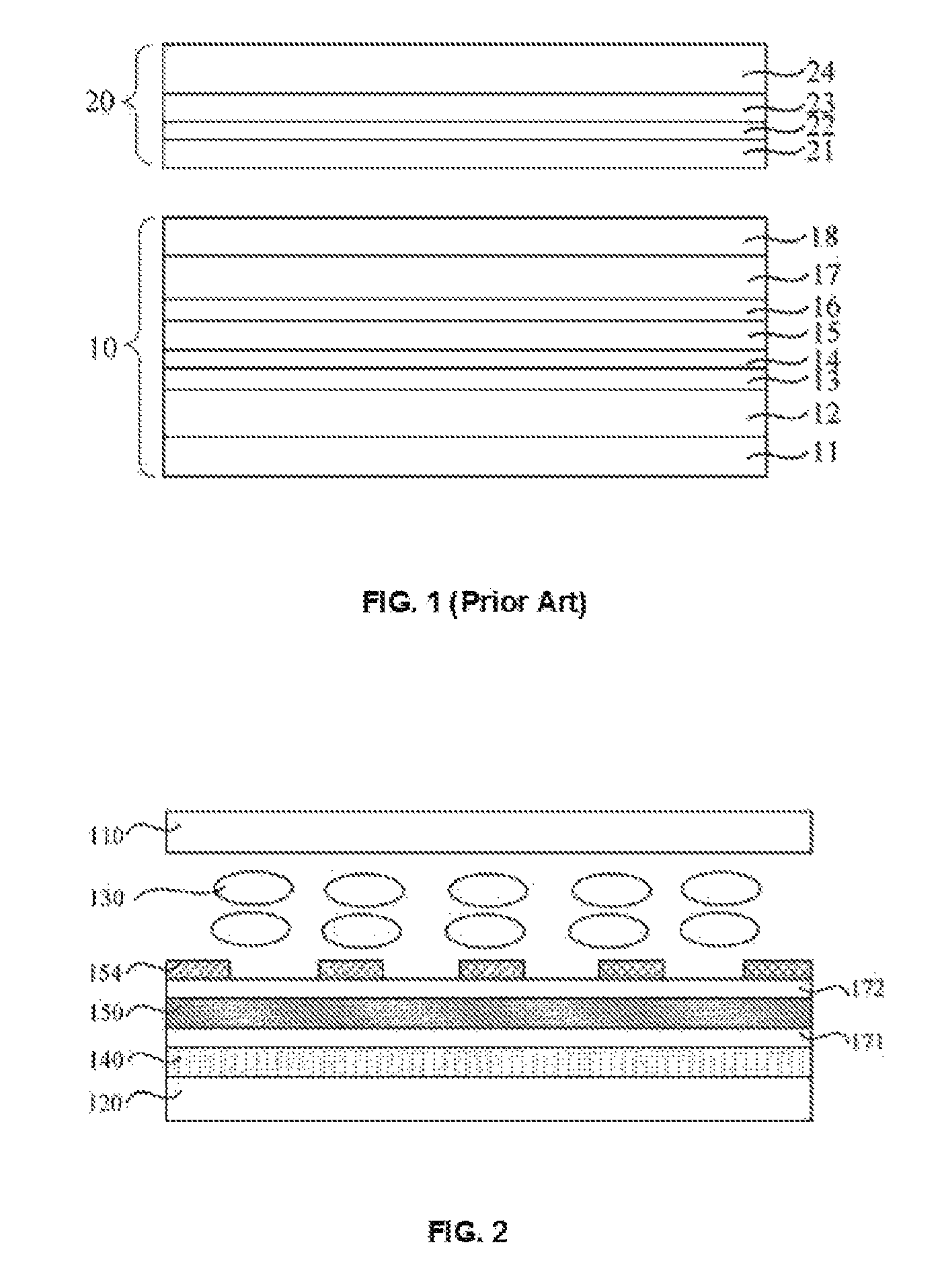
However, such a way that the touch panel 20 and the LCD panel 10 are manufactured separately and then assembled together will inevitably increase the thickness of the touch panel LCD device, resulting in a complicated display system and a complex manufacturing process, as well as high costs.
Furthermore, although the transparent shielding layer 21 can effectively shield the impact on the touch panel 20 by the electric noise of the LCD panel 10, the provision of the Indium Tin Oxide (ITO) layer not only increases the difficulty of the manufacturing process, but also increases the overall thickness of the whole device, thereby negatively affecting the trend of lightening and thinning of the device.

Method used


Image

  • Embedded touch screen liquid crystal display device and touch drive method thereof
  • Embedded touch screen liquid crystal display device and touch drive method thereof
  • Embedded touch screen liquid crystal display device and touch drive method thereof

Examples


first embodiment

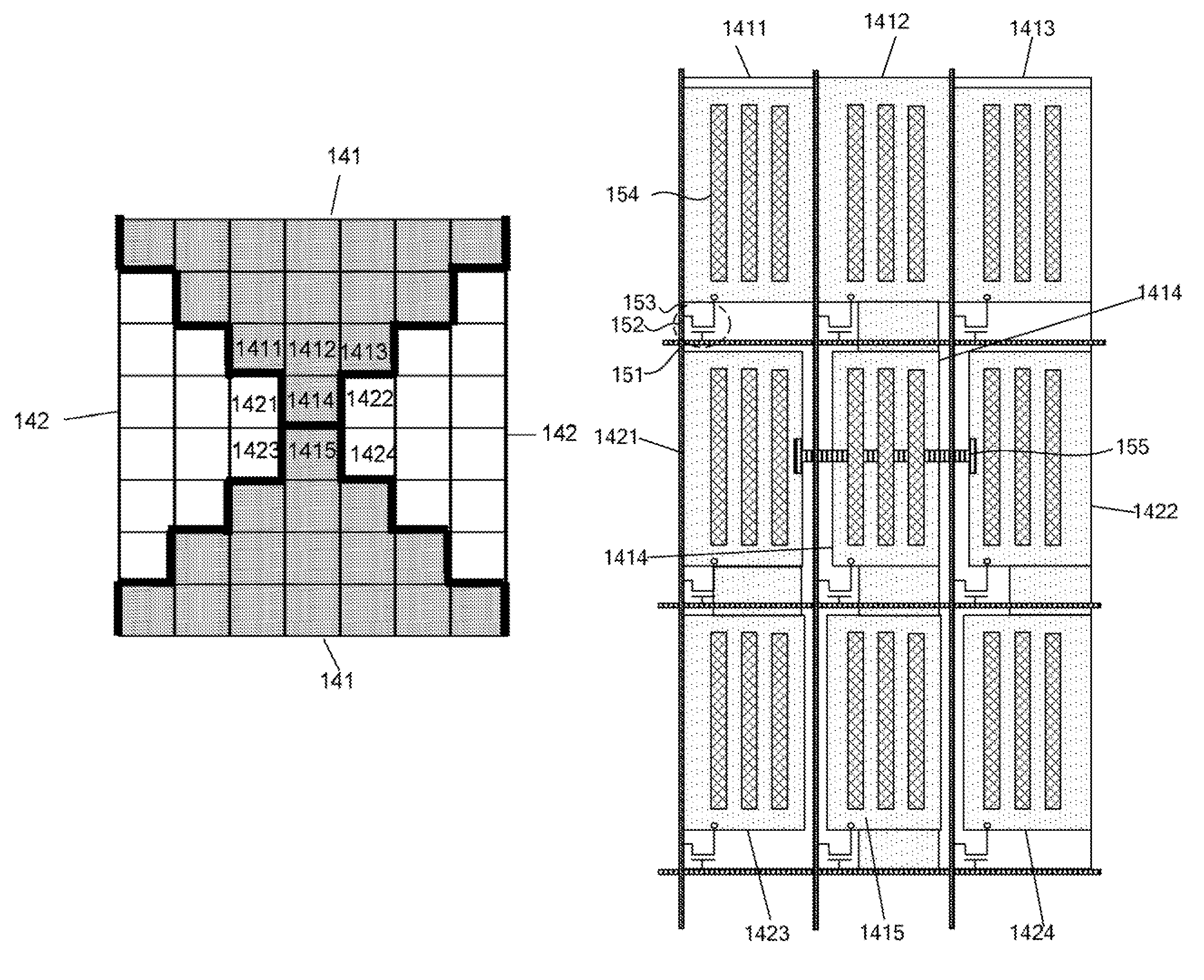
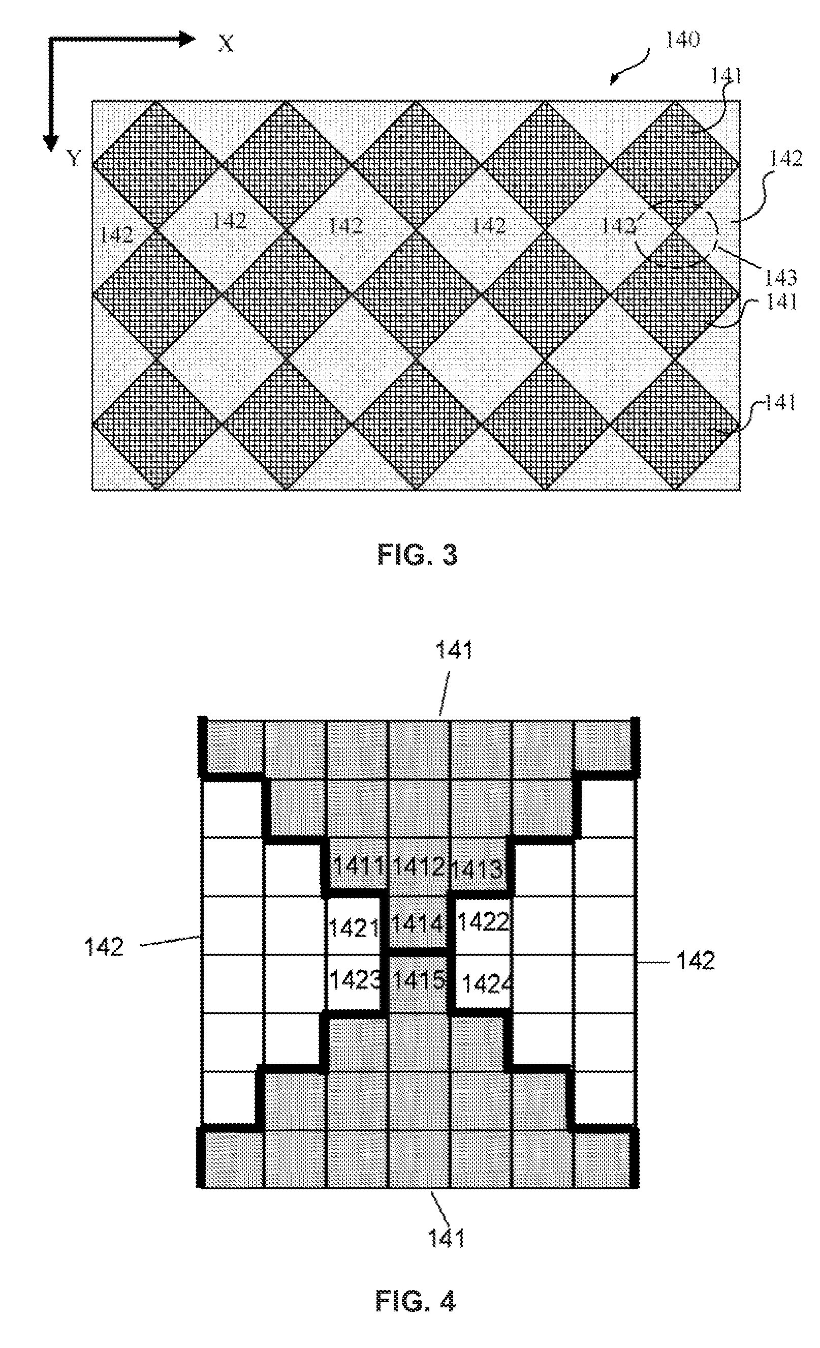
[0023]As shown in FIGS. 2 to 5, an in-cell touch panel liquid crystal display device of the first embodiment includes:

[0024]a first substrate 110 and a second substrate 120 disposed opposite to each other;

[0025]a liquid crystal layer 130 disposed between the first substrate 110 and the second substrate 120; and

[0026]a common electrode layer 140 disposed on a side of the second substrate 120 that faces the first substrate 110;

[0027]where the common electrode layer 140 includes a plurality of first common electrodes 141 and a plurality of second common electrodes 142 both arranged in a matrix, with the first common electrodes 141 and the second common electrodes 142 being configured for detecting a touched position on the in-cell touch panel liquid crystal display device.

[0028]In the first embodiment, the first substrate 110 is provided at the top and the second substrate 120 is provided at the bottom. A user can view the display of the liquid crystal display device from a side of the...

second embodiment

[0046]The adjacent two first common electrodes in each row are connected in the direction X by directly connected common electrodes of adjacent pixel units, and the adjacent two second common electrodes in each row are connected in the direction Y by the metal bridges 255 each connecting the common electrodes of two vertically adjacent pixel units. Similarly, the metal bridge 255 may be implemented in various ways, such as by etching a separate layer of metal to form the metal bridge. However, in the second embodiment, the existing metal layer is utilized. Specifically, to provide the metal bridges in the direction Y, a metal layer in the same layer with the data lines is used, because the data lines are also provided in the direction Y.

[0047]The operating manner of the in-cell touch panel liquid crystal display device in the second embodiment is the same as that in the first embodiment, and therefore is not described in detail here, but should be understood by those skilled in the ...

third embodiment

[0050]Specifically as shown in FIG. 9, the in-cell touch panel liquid crystal display device of the third embodiment includes:

[0051]a first substrate 310 and a second substrate 320 disposed opposite to each other;

[0052]a liquid crystal layer 330 disposed between the first substrate 310 and the second substrate 320; and

[0053]a common electrode layer 340 disposed on a side of the second substrate 320 that faces the first substrate 310;

[0054]where the common electrode layer 340 includes a plurality of first common electrodes and a plurality of second common electrodes both arranged in a matrix, with the first common electrodes and the second common electrodes being configured for detecting a touched position on the in-cell touch panel liquid crystal display device.

[0055]Furthermore, the in-cell touch panel liquid crystal display device further includes a TFT layer 350 which is disposed on a side of the second substrate 320 that faces the first substrate 310, the TFT layer 350 includes ...


PUM

PropertyMeasurementUnit
weightaaaaaaaaaa
transmittanceaaaaaaaaaa
coloraaaaaaaaaa

Abstract

An in-cell touch panel liquid crystal display device is disclosed. The display device includes a first substrate, a second substrate disposed opposite the first substrate, and a liquid crystal layer disposed between the first substrate and the second substrate. The display device also includes a common electrode layer disposed on a side of the second substrate facing the first substrate, where the common electrode layer includes a plurality of first common electrodes and a plurality of second common electrodes both arranged in a matrix. In addition, the first common electrodes and the second common electrodes are configured to detect a touched position on the in-cell touch panel liquid crystal display device.

Description

CROSS-REFERENCES TO RELATED APPLICATIONS[0001]This application is a U.S. national phase application of co-pending international patent application number PCT / CN2012 / 081426, filed Sep. 14, 2012 and entitled “IMBEDDED TOUCH SCREEN LIQUID CRYSTAL DISPLAY DEVICE AND TOUCH DRIVE METHOD THEREOF”, which claims priority to Chinese patent application number 201110383654.3, filed Nov. 25, 2011 and entitled “IMBEDDED TOUCH SCREEN LIQUID CRYSTAL DISPLAY DEVICE AND TOUCH DRIVE METHOD THEREOF”, the contents of which are incorporated herein by reference in their entirety.TECHNICAL FIELD[0002]The present invention relates to the field of liquid crystal displays, in particular to an in-cell touch panel liquid crystal display device and a touch driving method thereof.BACKGROUND OF THE INVENTION[0003]Due to its advantages such as light weight and thinness, a Liquid Crystal Display (LCD) device has gradually developed as one of the fastest growing flat panel displays. The LCD device displays images usi...

Claims


Application Information

Patent Timeline
Patent Type & Authority Patents(United States)
IPC IPC(8): G02F1/1343G06F3/044G06F3/041G02F1/1362G02F1/1333
CPCG02F1/134336G02F1/13338G06F3/0412G02F1/136286G06F3/044G06F2203/04103G06F2203/04111G06F3/0446G06F3/0443
Inventor HUO, SITAO
Owner SHANGHAI TIANMA MICRO ELECTRONICS CO LTD
Learn More