Semiconductor device and method for manufacturing the semiconductor device
a semiconductor and semiconductor technology, applied in the field of semiconductor devices, can solve the problems of difficult display recognition and difficult display recognition in the environment with strong external light, and achieve the effect of low power consumption
- Summary
- Abstract
- Description
- Claims
- Application Information
AI Technical Summary
Benefits of technology
Problems solved by technology
Method used
Image

Examples
embodiment 1
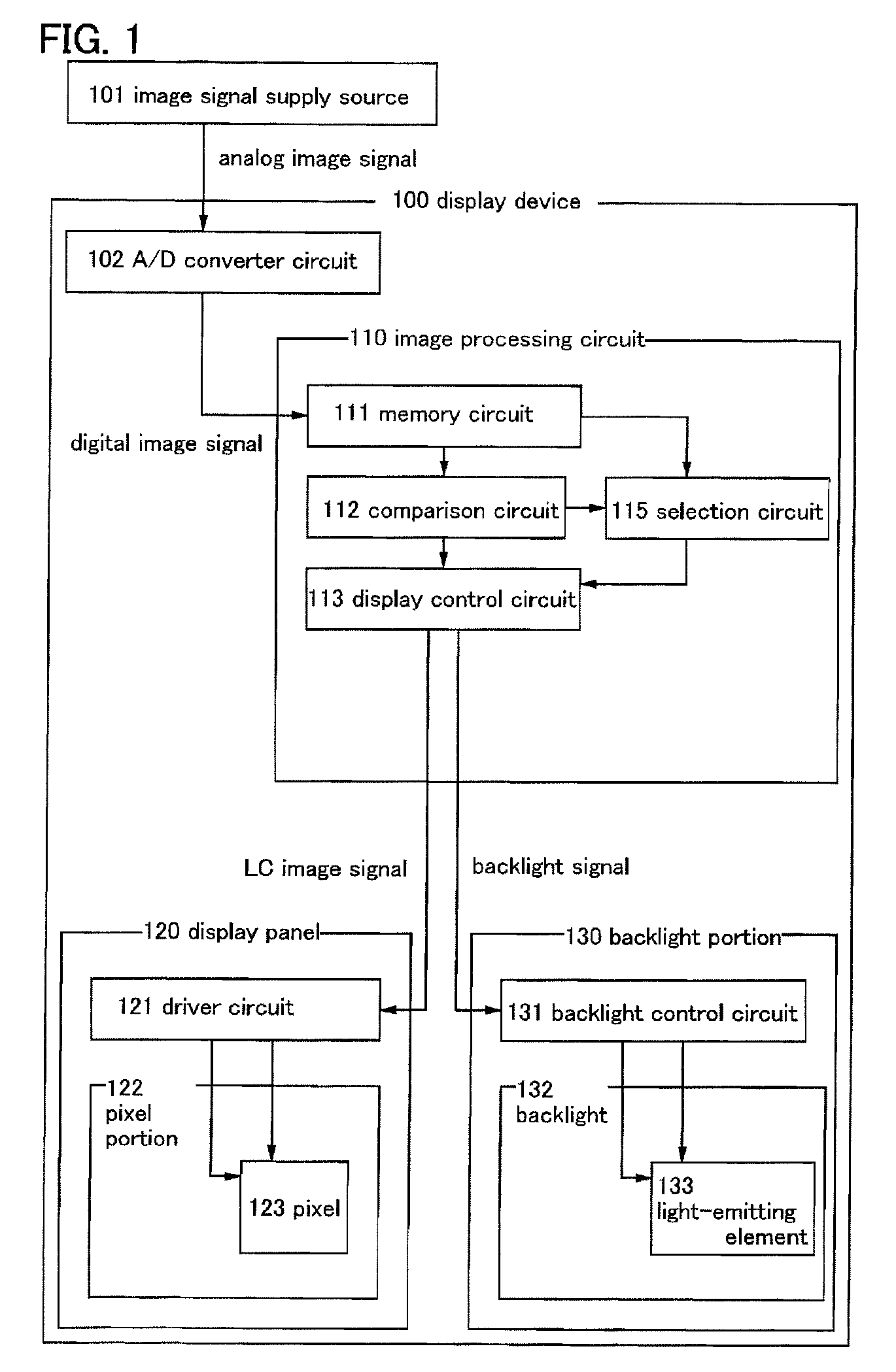
[0044]In this embodiment, a liquid crystal display device including a still-image mode and a moving-image mode is described with reference to FIG. 1. Note that in this specification, a mode performed in such a way that a display device determines image signals input to the display device as a still image is described as a still-image mode, and a mode performed in such a way that the display device determines the image signals input to the display device as a moving image is described as a moving-image mode.
[0045]A display device 100 of this embodiment includes an A / D converter circuit 102, an image processing circuit 110, a display panel 120, and a backlight portion 130 (see FIG. 1).
[0046]The image processing circuit 110 includes a memory circuit 111, a comparison circuit 112, a display control circuit 113, and a selection circuit 115.
[0047]The display panel 120 includes a driver circuit portion 121 and a pixel portion 122. In the pixel portion 122, a plurality of pixels 123 each co...
embodiment 2
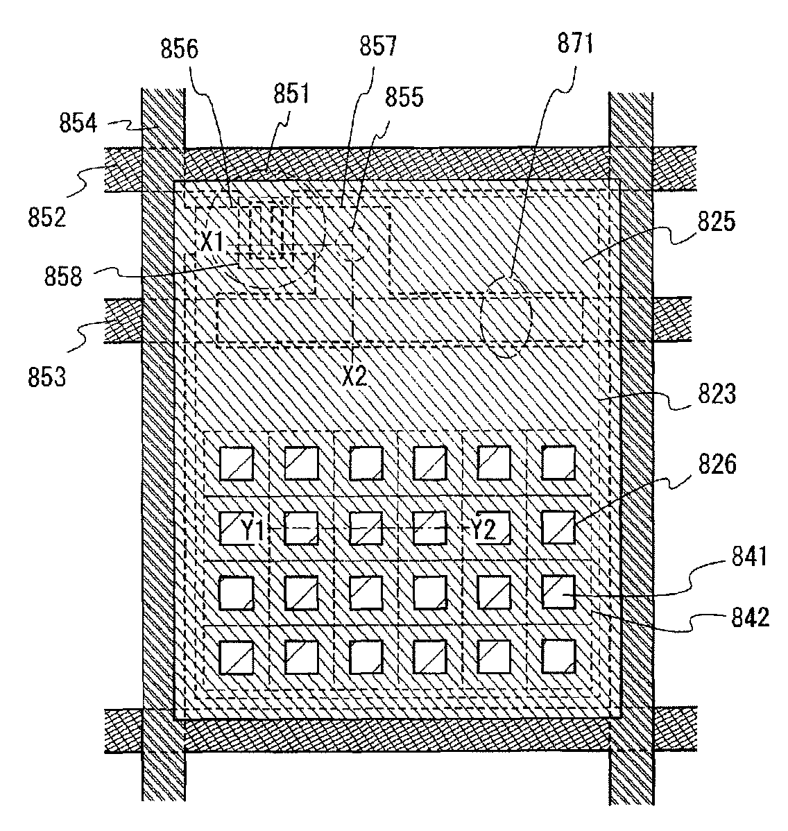
[0077]In this embodiment, a driving method of a liquid crystal display device is described using a pixel connection diagram, a timing chart, and the like. First, FIG. 2 is a schematic view of a display panel of a liquid crystal display device. In FIG. 2, the display panel includes a pixel portion 201, a scan line 202 (also referred to as a gate line), a signal line 203 (also referred to as a data line), a pixel 210, a common electrode 218, a capacitor line 219, a scan line side driver circuit 206, and a signal line side driver circuit 207.
[0078]The pixel 210 includes a pixel transistor 212, a liquid crystal element 213, and a capacitor 214. A gate of the pixel transistor 212 is connected to the scan line 202, a first terminal serving as one of a source and a drain of the pixel transistor 212 is connected to the signal line 203, and a second terminal serving as the other of the source and the drain of the pixel transistor 212 is connected to one electrode of the liquid crystal elemen...
embodiment 3
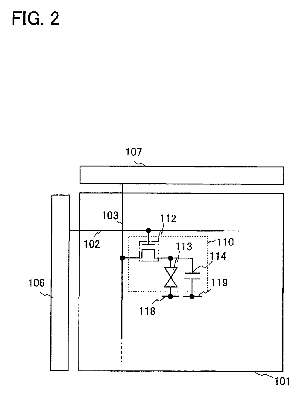
[0098]FIG. 4 illustrates a structure of a liquid crystal display module 190. The liquid crystal display module 190 includes a backlight portion 130, a color filter provided in a position overlapping with the backlight portion 130, a display panel 120 in which liquid crystal elements are arranged in a matrix, and a polarizing plate 125a and a polarizing plate 125b which are provided with the display panel 120 positioned therebetween. The backlight portion 130 is a surface-emitting backlight portion which emits uniform white light. For example, the backlight portion 130 may include a white light-emitting element 133 placed in an end portion of a light guide plate and a diffusing plate 134 provided between the light guide plate and the display panel 120. In addition, a flexible printed circuit (FPC) 126 serving as an external input terminal is electrically connected to a terminal portion provided in the display panel 120.
[0099]In FIG. 4, light 135 of three colors is schematically denot...
PUM
| Property | Measurement | Unit |
|---|---|---|
| angle | aaaaa | aaaaa |
| angle | aaaaa | aaaaa |
| distance | aaaaa | aaaaa |
Abstract
Description
Claims
Application Information
 - R&D
- Intellectual Property
- Life Sciences
- Materials
- Tech Scout
- Unparalleled Data Quality
- Higher Quality Content
- 60% Fewer Hallucinations
Browse by: Latest US Patents, China's latest patents, Technical Efficacy Thesaurus, Application Domain, Technology Topic, Popular Technical Reports.
© 2025 PatSnap. All rights reserved.Legal|Privacy policy|Modern Slavery Act Transparency Statement|Sitemap|About US| Contact US: help@patsnap.com