Guided-wave photodiode using through-absorber quantum-well-intermixing and methods thereof

Active Publication Date: 2016-10-25
NAT TECH & ENG SOLUTIONS OF SANDIA LLC
View PDF7 Cites 3 Cited by
  • Summary
  • Abstract
  • Description
  • Claims
  • Application Information

AI Technical Summary

Benefits of technology

[0006]Accordingly, the present invention includes a high-speed, high-saturation power detector (e.g., a photodiode) compatible with a relatively simple monolithic integration process. The photodiode includes an intrinsic bulk absorption region, which is grown above a main waveguide core including a number of quantum wells (QWs) that are used as the active region of a phase modulator. Through-absorber quantum-well-intermixing is used to blue-shift the bandedge of the

Problems solved by technology

Such coupling techniques can result in optical loss, costly packaging required for

Method used


Image

  • Guided-wave photodiode using through-absorber quantum-well-intermixing and methods thereof
  • Guided-wave photodiode using through-absorber quantum-well-intermixing and methods thereof
  • Guided-wave photodiode using through-absorber quantum-well-intermixing and methods thereof

Examples


example

Example 1

Integrated Guided-Wave Photodiode Using Through-Absorber Quantum-Well-Intermixing

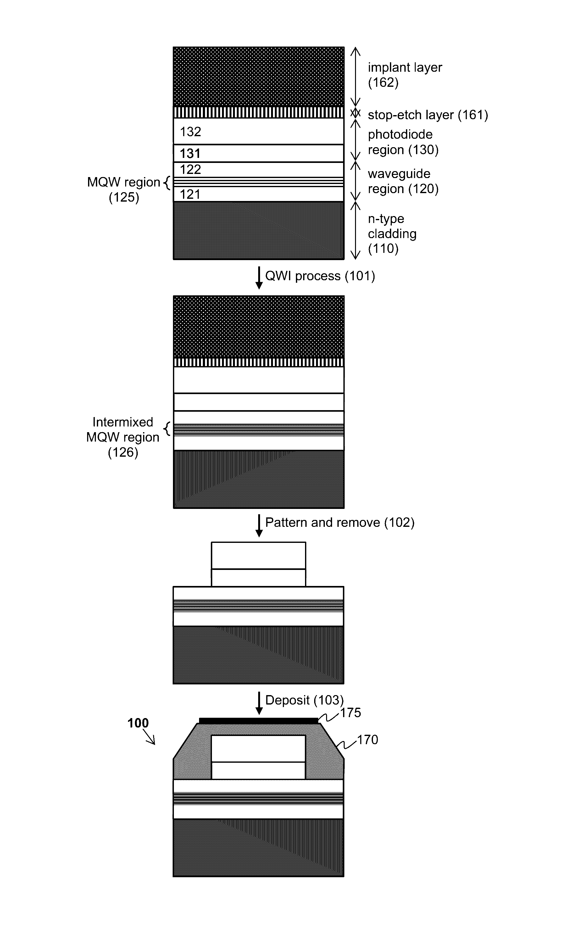
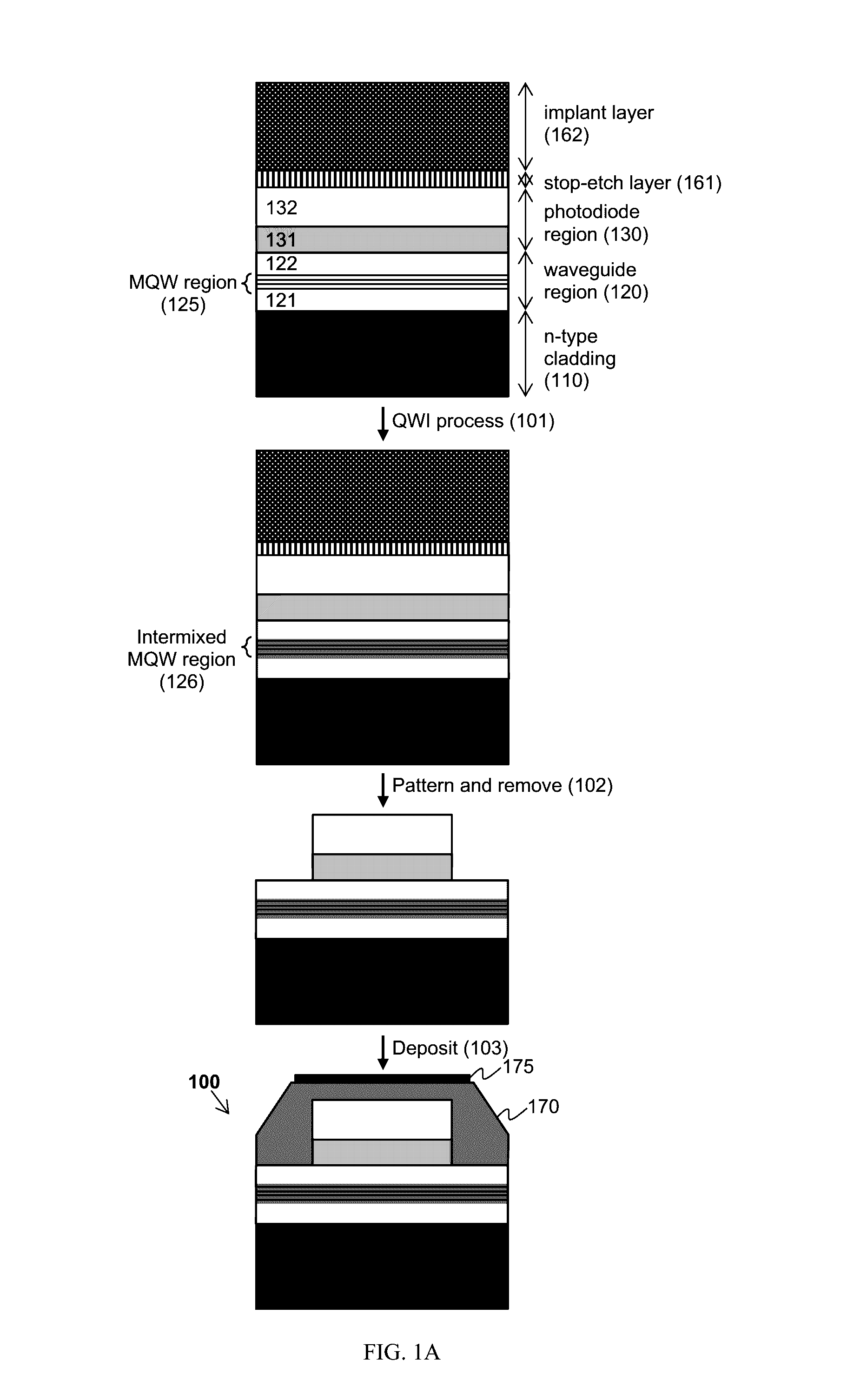
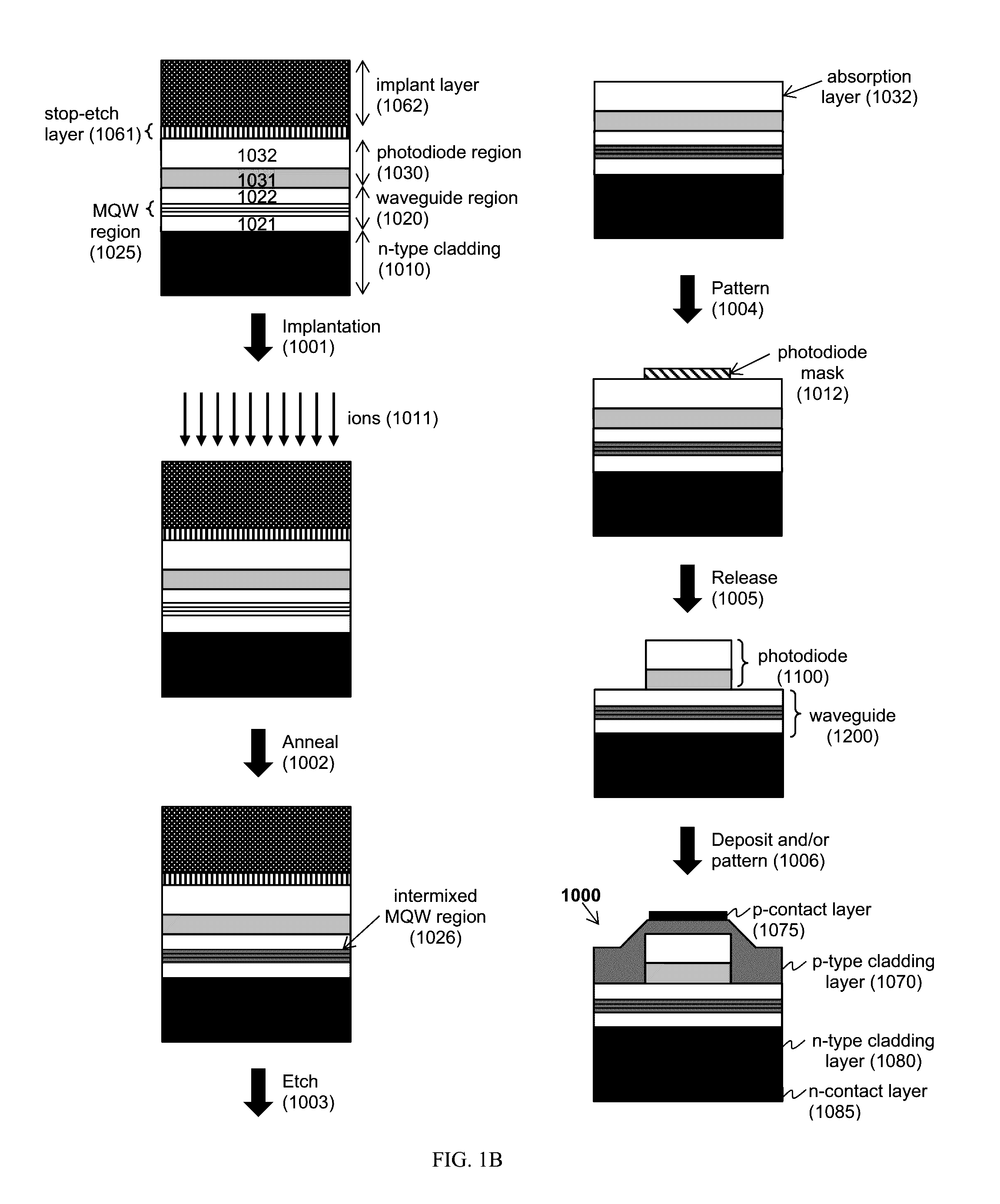
[0076]Monolithic integration of optoelectronic components have been pursued for many applications due to the potential to not only reduce size, weight, and power of such systems, but also to enable new functionality which cannot be emulated by discrete components. Quantum-well-intermixing (QWI) has been shown to be a powerful technique to enable the integration of many optoelectronic components including semiconductor lasers, amplifiers, attenuators, photodiodes, electro-absorption modulators, active ring-resonators, and various low-loss waveguide components (see, e.g., Skogen E J et al., “Optical AND and NOT gates at 40 Gbps using electro-absorption modulator / photodiode pairs,”Proc. 23rd Annual Meeting of the IEEE Photonics Soc., held on 7-11 Nov. 2010 in Denver, Colo., pp. 52-3; and Tauke-Pedretti A et al., “Mutual injection locking of monolithically integrated coupled-cavity DBR lasers,”IEEE...


PUM


Abstract

The present invention includes a high-speed, high-saturation power detector (e.g., a photodiode) compatible with a relatively simple monolithic integration process. In particular embodiments, the photodiode includes an intrinsic bulk absorption region, which is grown above a main waveguide core including a number of quantum wells (QWs) that are used as the active region of a phase modulator. The invention also includes methods of fabricating integrated photodiode and waveguide assemblies using a monolithic, simplified process.

Description

CROSS-REFERENCE TO RELATED APPLICATION[0001]This application claims the benefit of U.S. Provisional Application No. 62 / 025,656, filed Jul. 17, 2014, which is hereby incorporated by reference in its entirety.STATEMENT OF GOVERNMENT INTEREST[0002]This invention was made with Government support under contract no. DE-AC04-94AL85000 awarded by the U.S. Department of Energy to Sandia Corporation. The Government has certain rights in the invention.FIELD OF THE INVENTION[0003]The present invention relates to integrated optoelectronic (e.g., photodiode) structures and methods for making and using such structures.BACKGROUND OF THE INVENTION[0004]Monolithic integration of optoelectronic components can provide numerous benefits, including reductions in size, cost, weight, and power dissipation, as well as new functionality that cannot be emulated by discrete components. For instance, when discrete components are used, these components must be coupled (e.g., using an optical fiber or optical spl...

Claims


Application Information

Patent Timeline
IPC IPC(8): H01L31/0232H01L31/0352G02B6/134H01L31/18G02B6/132G02B6/12
CPCG02B6/132H01L31/1844H01L31/02327H01L31/035272G02B6/1347G02B2006/12128G02B2006/12123H01L31/105H01L31/109
Inventor SKOGEN, ERIK J.
Owner NAT TECH & ENG SOLUTIONS OF SANDIA LLC
Why Eureka
Try Eureka