Nitride semiconductor device and method for producing the same

a technology of nitride and semiconductor layers, which is applied in the direction of semiconductor devices, basic electric elements, electrical appliances, etc., can solve the problems of requiring a long time to form these layers, and achieve the effects of reducing crystal defects in the nitride semiconductor layers, high quality, and reducing crystal defects

Active Publication Date: 2016-12-06
NICHIA CORP
View PDF23 Cites 4 Cited by
  • Summary
  • Abstract
  • Description
  • Claims
  • Application Information

AI Technical Summary

Benefits of technology

[0008]In other words, in the conventional production processes, the semiconductor stack, buffer layer and underlayer combined, needs to have a considerably large thickness, requiring a long time to form these layers. One object of the present disclosure is to provide a nitride semiconductor device that can be produced in a simplified manner and has reduced crystal defects in the nitride semiconductor layers, and provide a method for producing the same.
[0011]The method for producing a nitride semiconductor device according to the present disclosure can produce a nitride semiconductor device with reduced crystal defects in the nitride semiconductor layers in a simplified manner.
[0012]The nitride semiconductor device according to the present disclosure can be of high quality with reduced crystal defects in the nitride semiconductor layers.

Problems solved by technology

In other words, in the conventional production processes, the semiconductor stack, buffer layer and underlayer combined, needs to have a considerably large thickness, requiring a long time to form these layers.

Method used


Image

  • Nitride semiconductor device and method for producing the same
  • Nitride semiconductor device and method for producing the same
  • Nitride semiconductor device and method for producing the same

Examples


Embodiment Construction

[0038]Various embodiments of the present invention will be explained below, with some references to accompanying drawings.

[0039]The drawings referenced in the explanation below are schematic representations of some embodiments of the present invention. As such, the objects might not be drawn to scale, their spacing and relative positions may be exaggerated, or a part of an object might be omitted. Moreover, scaling or spacing of the objects might not match between the plan and sectional views. In the explanation below, moreover, those having the same designations and reference numerals are of the same member or the same material as a rule, for which detailed explanations are omitted as deemed appropriate.

Configuration of Nitride Semiconductor Device

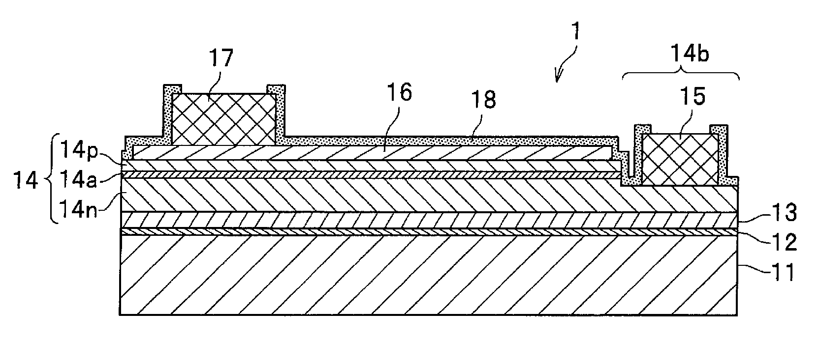
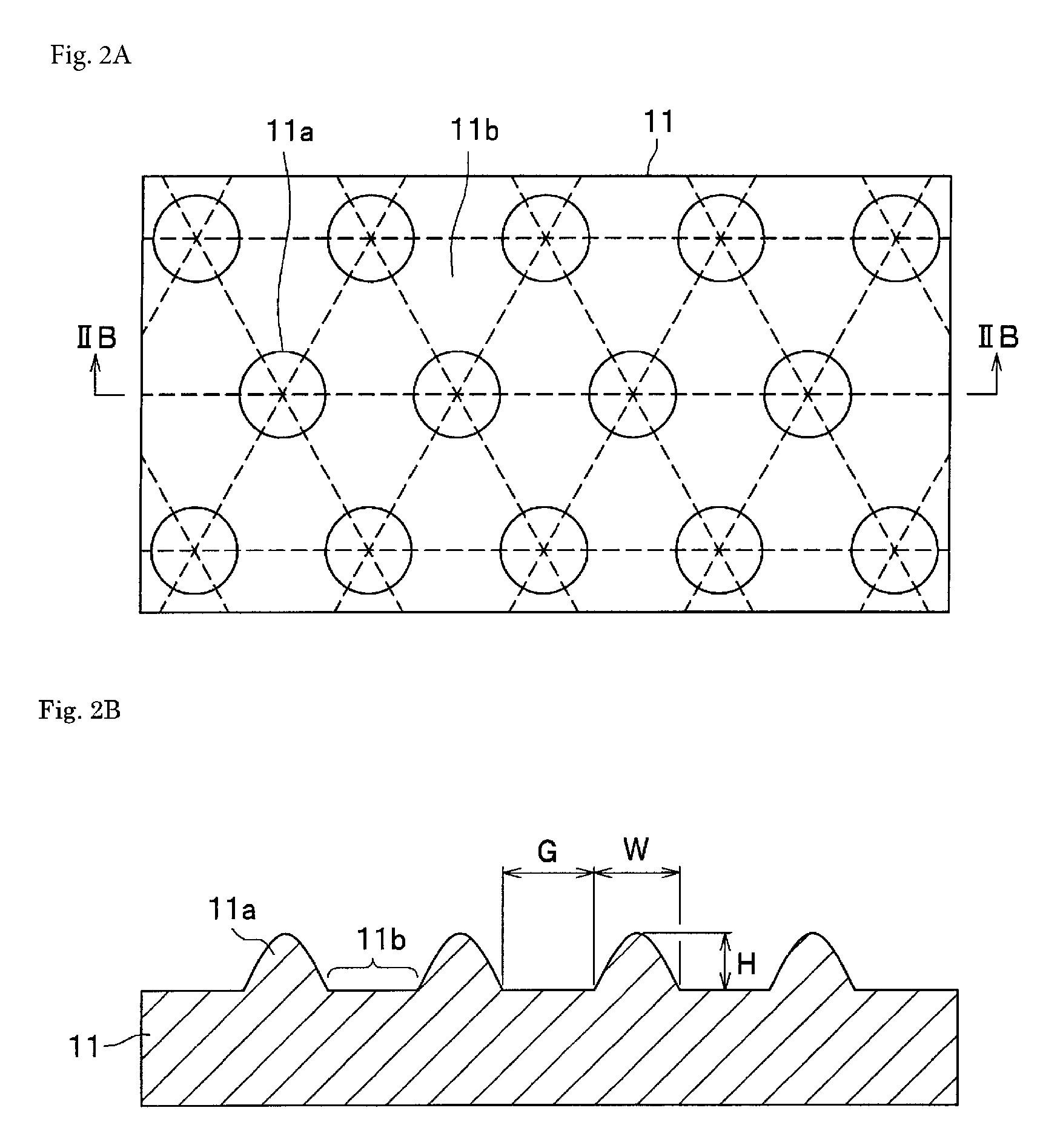
[0040]The configuration of a nitride semiconductor device according to one embodiment will be explained with reference to FIGS. 1, 2A and 2B. FIG. 1 is a schematic cross-sectional view illustrating a configuration of a nitride semiconduct...


PUM


Abstract

A method for producing a nitride semiconductor device. The method comprises providing a substrate made of a material other than a nitride semiconductor. The material has a hexagonal crystal structure. An upper face of the substrate has at least one flat section. The method further comprises growing a first nitride semiconductor layer on the upper face of the substrate. The first nitride semiconductor layer is made of monocrystalline AlN. The first nitride semiconductor layer has an upper face that is a +c plane. The first nitride semiconductor layer has a thickness in a range of 10 nm to 100 nm. The method further comprises growing a second nitride semiconductor layer on the upper face of the first nitride semiconductor layer. The second nitride semiconductor layer is made of InXAlYGa1-X-YN (0≦X, 0≦Y, X+Y<1). In an initial stage of growing the second nitride semiconductor layer, micronuclei are formed in multiple locations on the upper face of the first nitride semiconductor layer such that a plurality of upside-down hexagonal pyramid-shaped or upside-down hexagonal frustum-shaped recesses separate the micronuclei above the at least one flat section of the upper face of the substrate. After the initial stage of growing, further growth is performed to reduce a size of the recesses until the recesses are substantially eliminated. The further growth is performed such that the recesses are substantially eliminated before a thickness of the second nitride semiconductor layer grows to 800 nm. The second nitride semiconductor layer is grown to have an upper face with at least one flat section.

Description

CROSS-REFERENCE TO RELATED APPLICATION[0001]This application claims priority to Japanese Patent Application No. 2014-233922, filed on Nov. 18, 2014. The entire disclosure of Japanese Patent Application No. 2014-233922 is hereby incorporated herein by reference.BACKGROUND[0002]1. Field of the Invention[0003]The present disclosure relates to a nitride semiconductor device and a method for producing the same.[0004]2. Description of Related Art[0005]A conventional process for producing nitride semiconductor devices involves forming a buffer layer made of a nitride, such as AlN, which moderates lattice constant mismatch, on a sapphire substrate or the like, and further stacking a gallium nitride-based semiconductor by metalorganic chemical vapor deposition. Japanese Patent Application Publication No. 2006-080378 and Japanese Patent Application Publication No. 2013-065849, for example, each discloses a process for stacking, as buffer layers, a first buffer layer made of high carbon concen...

Claims


Application Information

Patent Timeline
Patent Type & Authority Patents(United States)
IPC IPC(8): H01L21/00H01L33/12H01L33/00H01L33/32H01L21/02H01L33/16
CPCH01L33/007H01L21/0254H01L21/02433H01L21/02505H01L21/02609H01L21/02639H01L33/12H01L33/32H01L33/16H01L21/0242H01L21/0243H01L21/02458H01L21/02516H01L21/0262H01L21/02647H01L33/20H01L33/0075H01L33/18H01L33/24
Inventor MICHIUE, ATSUO
Owner NICHIA CORP
Why Eureka
Try Eureka