Semiconductor package and semiconductor module
- Summary
- Abstract
- Description
- Claims
- Application Information
AI Technical Summary
Benefits of technology
Problems solved by technology
Method used
Image

Examples
first embodiment
[0029](First Embodiment)
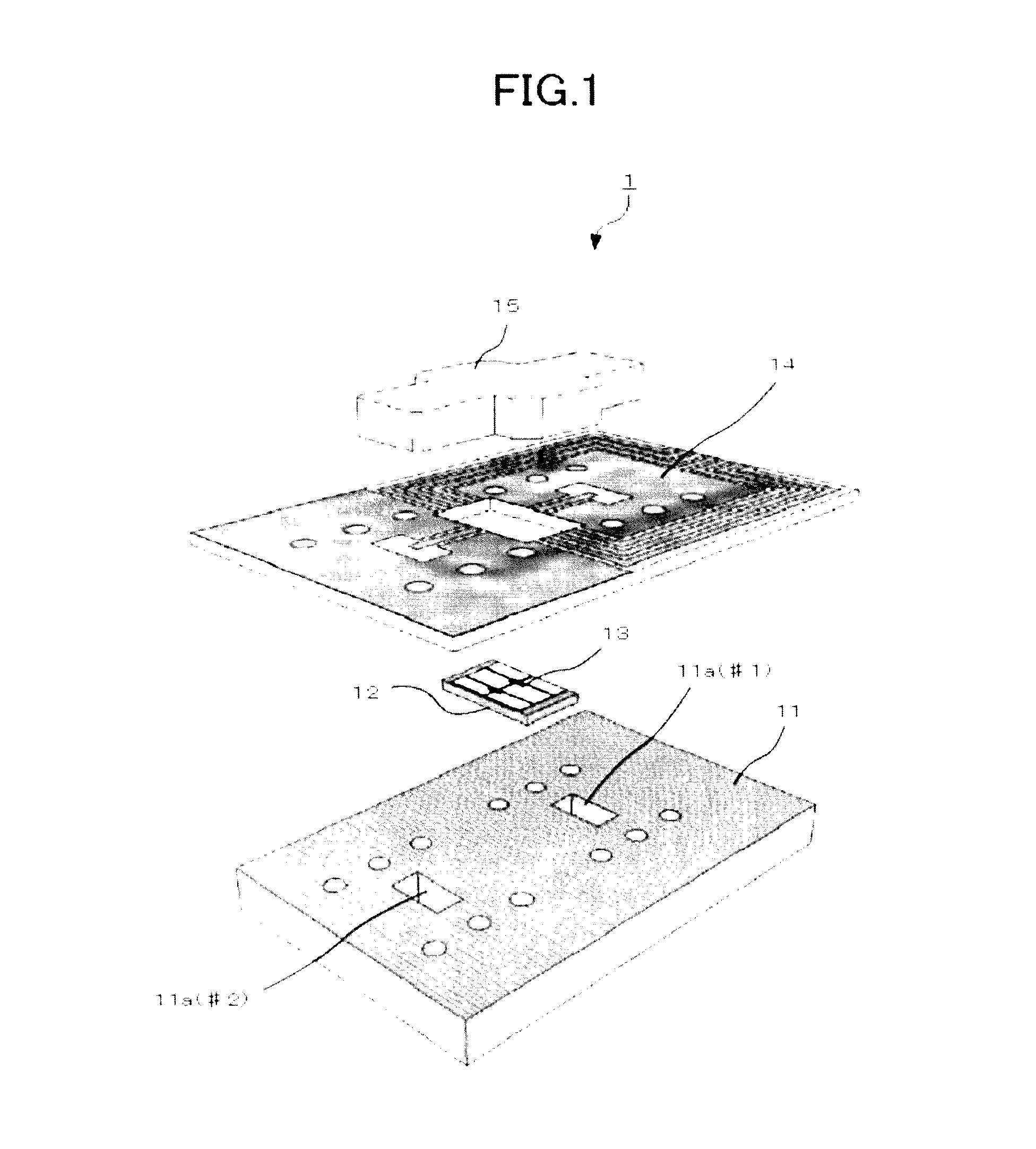
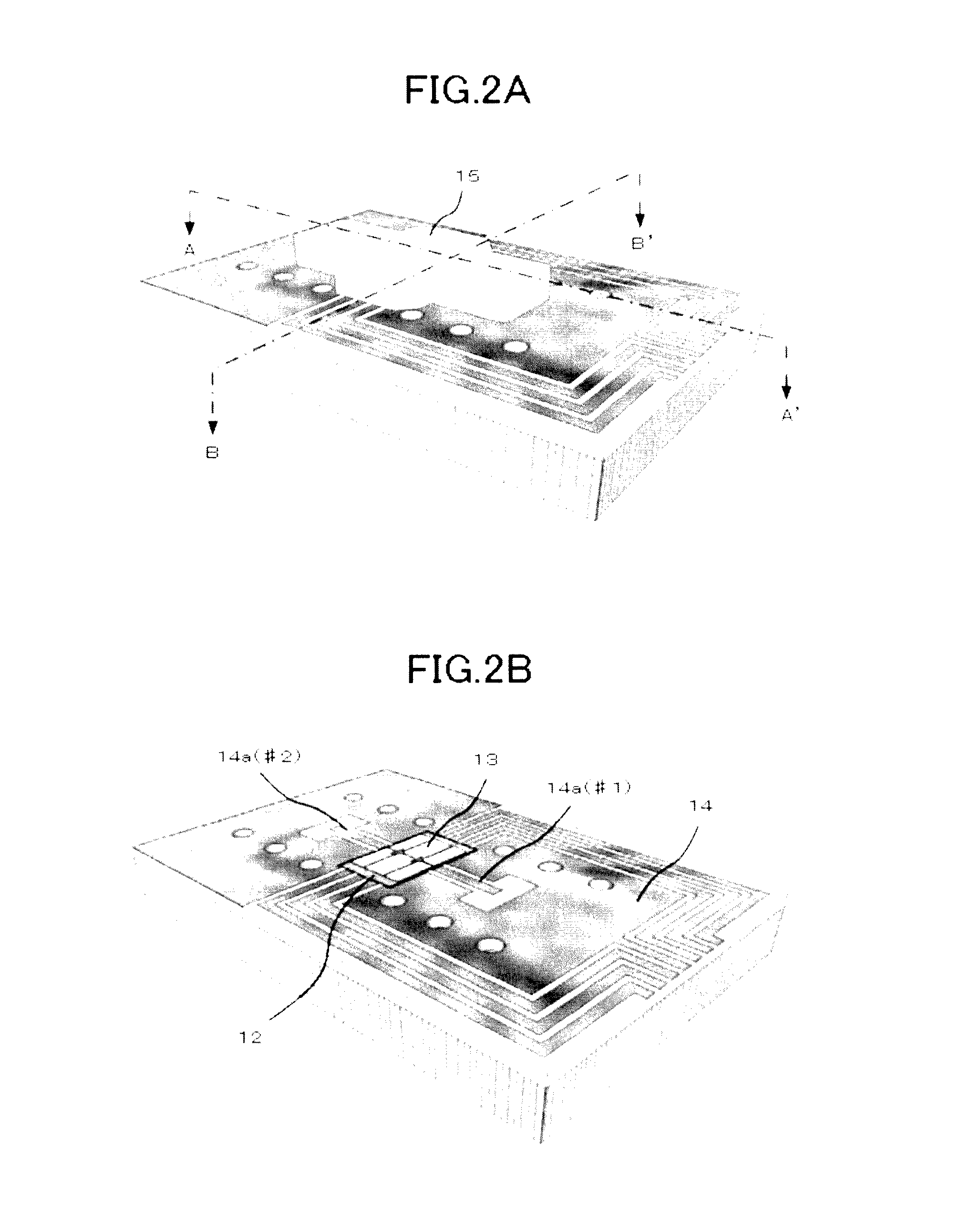
[0030]FIGS. 1 to 3D are views illustrating a semiconductor package according to a first embodiment. In all of the drawings, a semiconductor device 13 is housed inside the semiconductor package. The semiconductor device 13 is formed of a semiconductor chip. For example, the semiconductor device 13 is formed of a semiconductor chip for signal power amplification including a plurality of active devices (e.g., semiconductor device for signal amplification). Note that, in the following description, not only a semiconductor package not mounted with a semiconductor device but also a semiconductor package mounted with a semiconductor device will be referred to as “semiconductor package”. The semiconductor package mounted with the semiconductor device can also be referred to as “semiconductor module”.
[0031]As illustrated in FIGS. 1 to 3D, a semiconductor package 1 includes a waveguide interface metal plate 11 as a first metal body, a chip-mounting metal plate 12 as a ...
second embodiment
[0048](Second Embodiment)
[0049]FIG. 4 is an exploded perspective view illustrating a semiconductor package according to a second embodiment. A main section is illustrated in a transparent manner. A semiconductor device 23 is housed inside the semiconductor package. As illustrated in FIG. 4, a semiconductor package 2 includes a metal block 21 as a first metal body, a chip-mounting metal plate 22 as a second metal body, the semiconductor device 23, aline substrate 24, and a lid body 25 as a lid body.
[0050]The metal block 21 is a waveguide incorporated metal block inside which the waveguide path is formed. The waveguide path is a through-hole and forms a part of a back-short structure. The metal block 21 is formed of, for example, copper, aluminum, or alloy containing these metals. An external shape of the metal block 21 is a cuboid. The metal block 21 has respective surfaces formed flat. Inside the metal block 21, two independent waveguide paths 21a (21a (#1) and 21a (#2)) are formed ...
third embodiment
[0059](Third Embodiment)
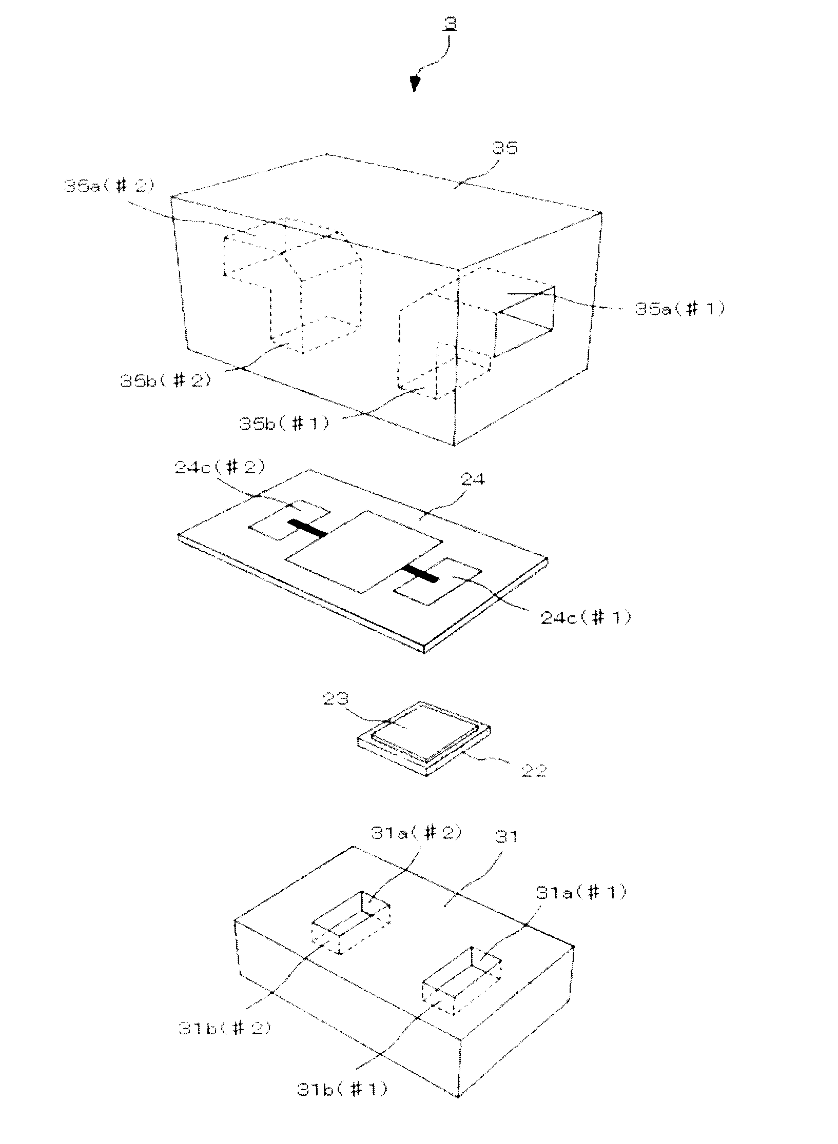
[0060]FIG. 5 is an exploded perspective view illustrating a semiconductor package according to a third embodiment. The portions identical to those in a semiconductor package according to a second embodiment are denoted by same reference signs. According to the second embodiment, a lowest layer of the semiconductor package is a metal block formed with a waveguide inside thereof, and a highest layer is a resin-made lid body formed with the back-short end. However, according to the third embodiment, the lowest layer of the semiconductor package is a metal block formed with a back-short end, and the highest layer is a resin-made lid body formed with the waveguide path inside thereof. In the following, a semiconductor package 3 according to the third embodiment will be described. Note that description that overlaps the second embodiment will be simplified.
[0061]In FIG. 5 also, a main section is illustrated in a transparent manner. A semiconductor device 23 is hous...
PUM
 Abstract
Description
Claims
Application Information
 - R&D
- Intellectual Property
- Life Sciences
- Materials
- Tech Scout
- Unparalleled Data Quality
- Higher Quality Content
- 60% Fewer Hallucinations
Browse by: Latest US Patents, China's latest patents, Technical Efficacy Thesaurus, Application Domain, Technology Topic, Popular Technical Reports.
© 2025 PatSnap. All rights reserved.Legal|Privacy policy|Modern Slavery Act Transparency Statement|Sitemap|About US| Contact US: help@patsnap.com