Inorganic light-emitting diode with encapsulating reflector

a light-emitting diode and organic technology, applied in the direction of solid-state devices, basic electric elements, electric devices, etc., can solve the problems of led inefficiency, micro-led structures useful for enabling such transfer printing processes not necessarily compatible with known light-extraction structures, and achieve the effect of improving efficiency and light outpu

Active Publication Date: 2017-01-03
X DISPLAY CO TECH LTD
View PDF132 Cites 58 Cited by
  • Summary
  • Abstract
  • Description
  • Claims
  • Application Information

AI Technical Summary

Benefits of technology

[0007]The present invention provides a light-emitting diode structure and manufacturing method that is compatible with micro transfer printing and has an increased efficiency and improved light output. The construction process is compatible with existing photolithographic processes and is suitable for making a large number of light-emitting diodes on a conventional wafer.

Problems solved by technology

Much of the light emitted from an LED is therefore trapped due to total internal reflection and is eventually converted to heat.
This phenomenon is one of the greatest causes of LED inefficiency.
However, micro-LED structures useful for enabling such transfer printing processes are not necessarily compatible with known light-extraction structures.

Method used


Image

  • Inorganic light-emitting diode with encapsulating reflector
  • Inorganic light-emitting diode with encapsulating reflector
  • Inorganic light-emitting diode with encapsulating reflector

Examples


Embodiment Construction

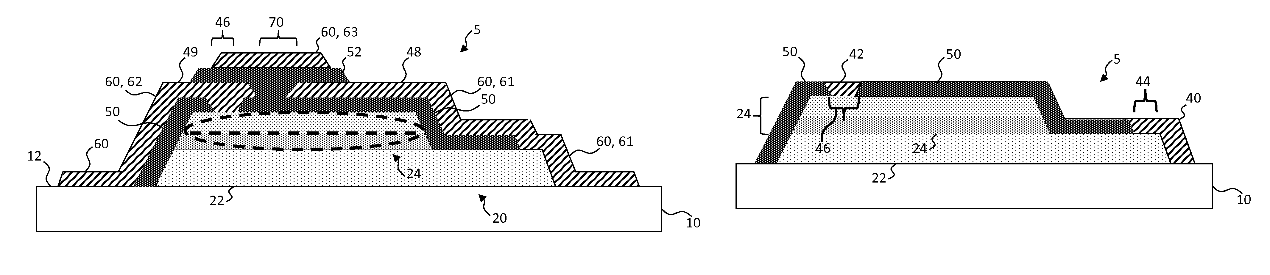
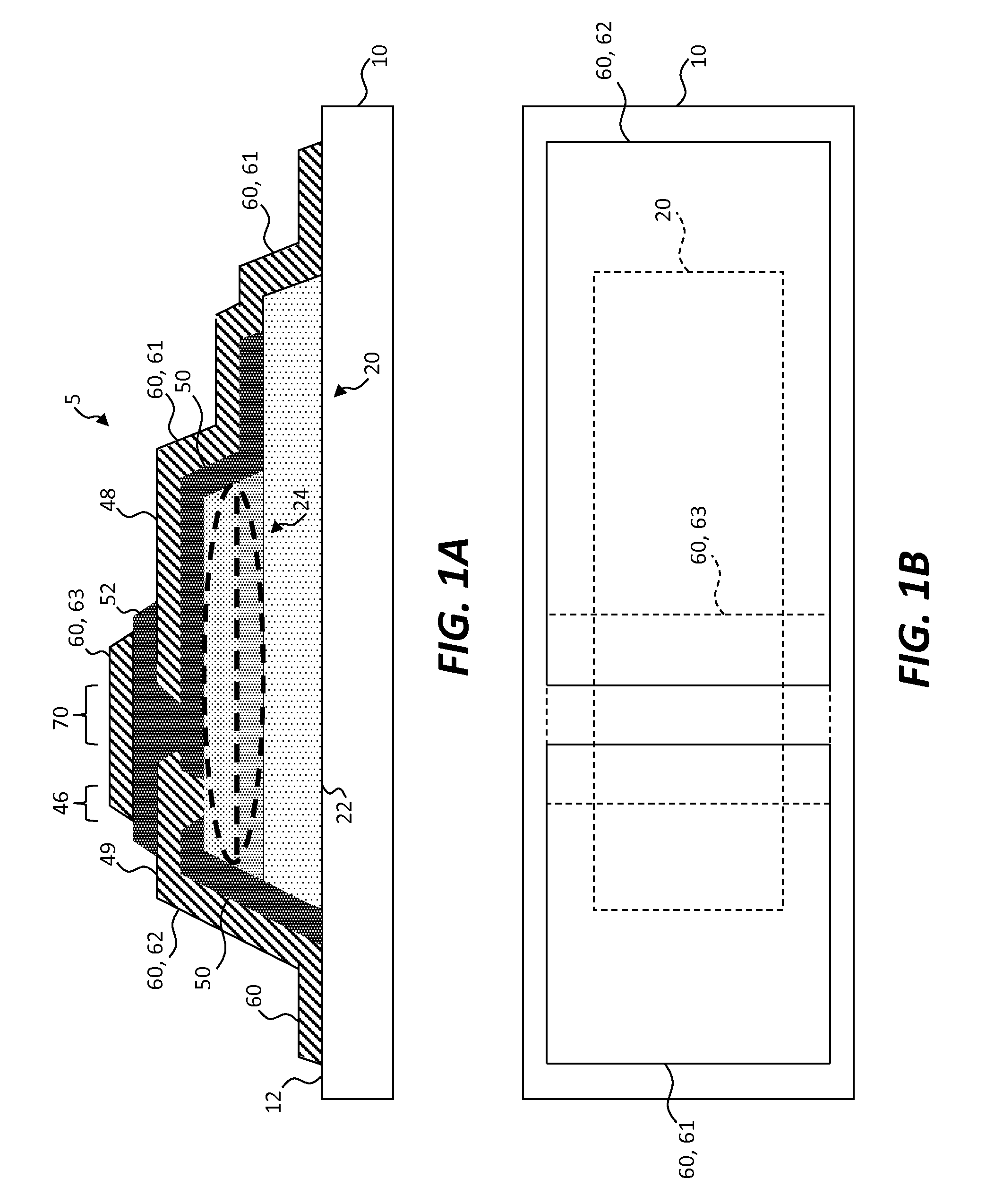
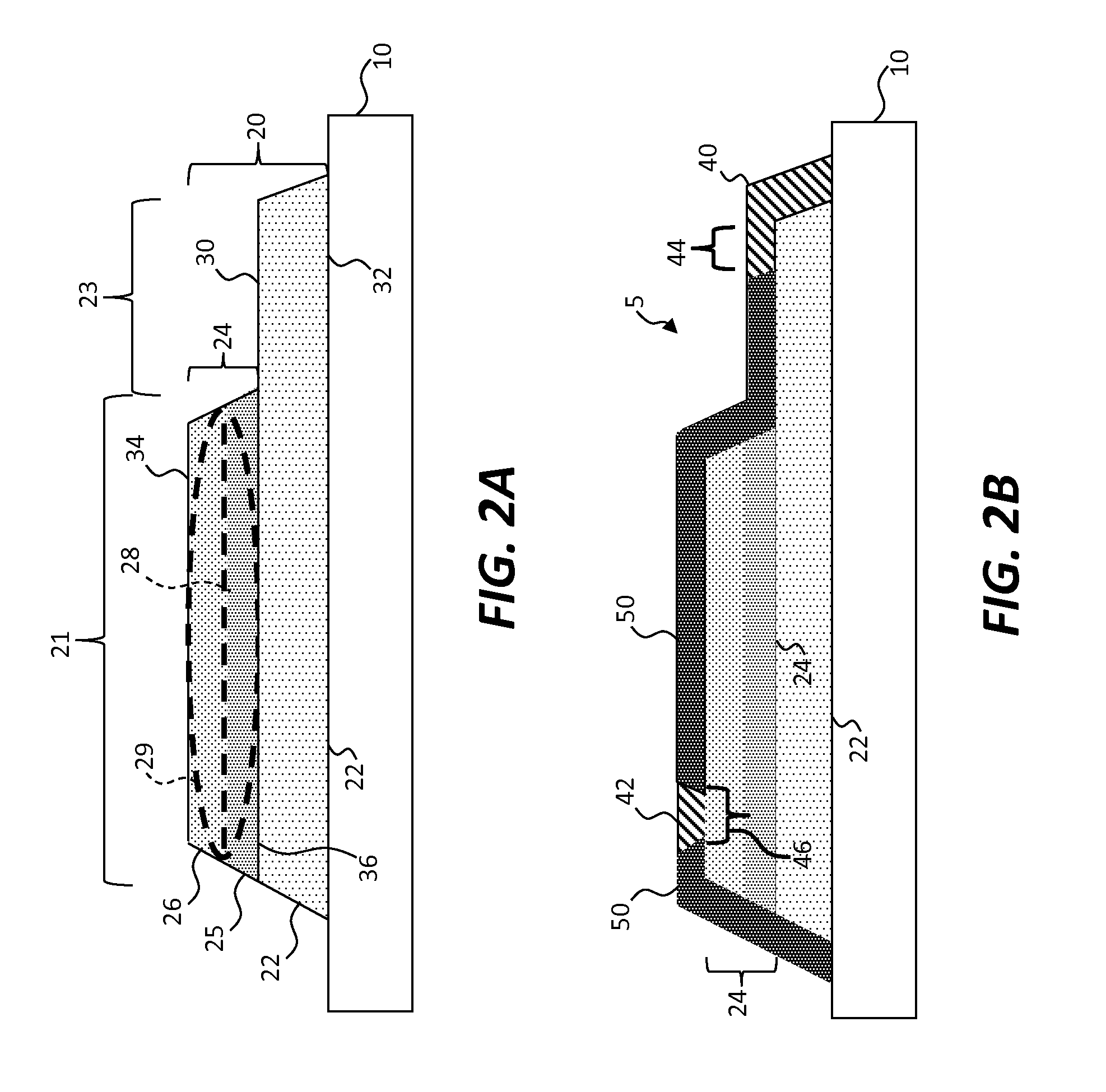
[0108]Referring to the cross section of FIG. 1A, the plan view of FIG. 1B, the detailed cross sections of FIGS. 2A, 2B and 3A, and the plan view of FIG. 3B, in an embodiment of the present invention, an inorganic light-emitting diode structure 5 includes a transparent substrate 10 having a transparent substrate surface 12 and an inorganic semiconductor structure 20 formed in a three-dimensional structure on the transparent substrate surface 12 of the transparent substrate 10. The three-dimensional inorganic semiconductor structure 20 includes a conduction layer 22 and a light-emitting layer 24 over and in contact with only a first portion 21 of the conduction layer 22 leaving a second portion 23 of the conduction layer 22 that is not covered by the light-emitting layer 24 (FIG. 2A). The light-emitting layer 24 and the conduction layer 22 each have first and second opposing sides 34, 36, 30, 32 (FIG. 2A), respectively. Only a portion of the first side 30 of the conduction layer 22 is...


PUM

PropertyMeasurementUnit
heightaaaaaaaaaa
heightaaaaaaaaaa
heightaaaaaaaaaa

Abstract

An inorganic light-emitting diode structure includes a transparent substrate and an inorganic semiconductor having a conduction layer and a light-emitting layer over and in contact with only a portion of the conduction layer. A first metal contact is in electrical contact with the conduction layer and a second metal contact is in electrical contact with a second contact portion of the light-emitting layer so that a current supplied between the first metal contact and the second metal contact through the inorganic semiconductor causes the light-emitting layer to emit light. A dielectric layer is located over at least a portion of the light-emitting layer and a reflective layer is located over at least a portion of the dielectric layer. The reflective layer encapsulates the light-emitting layer exclusive of the portion of the conduction layer in contact with the light-emitting layer.

Description

CROSS REFERENCE TO RELATED APPLICATIONS[0001]Reference is made to U.S. patent application Ser. No. 14 / 783,988 filed Jun. 18, 2015, entitled Micro-Assembled LED Displays and Lighting Elements, and U.S. Patent Application Ser. No. 62 / 055,472 filed Sep. 25, 2014, entitled Compound Micro-Assembly Strategies and Devices, the contents of each of which is incorporated by reference herein in its entirety.FIELD OF THE INVENTION[0002]The present invention relates to a light-emitting diode structure having an encapsulating reflector providing improved light output and efficiency.BACKGROUND OF THE INVENTION[0003]Inorganic light-emitting diodes (LEDs) are widely used in electronic devices as indicators and in displays. LEDs include a multi-layer doped crystalline semiconductor structure that responds to electrical current by emitting light. The frequency of the light emitted depends upon the bandgap and doping of the semiconductor. Electrical current is provided by a power supply connected to el...

Claims


Application Information

Patent Timeline
Patent Type & Authority Patents(United States)
IPC IPC(8): H01L33/60H01L33/54H01L33/38H01L27/15
CPCH01L33/60H01L27/156H01L33/54H01L33/38H01L33/46H01L33/405H01L33/385
Inventor BOWER, CHRISTOPHERMEITL, MATTHEW
Owner X DISPLAY CO TECH LTD
Why Eureka
Try Eureka