Method and system for fast inspecting defects

a defect inspection and defect technology, applied in the field of methods and systems for fast inspection of defects, can solve the problems of missing real defects, misjudging non-defects, and wasting time on repeated scanning, so as to save time for repeated scanning, improve accuracy, and improve accuracy

Active Publication Date: 2017-01-10
ASML NETHERLANDS BV
View PDF28 Cites 4 Cited by
  • Summary
  • Abstract
  • Description
  • Claims
  • Application Information

AI Technical Summary

Benefits of technology

[0008]The present invention is directed to a method and system for inspecting defects which saves scanned raw data as an original image so as to save time for repeated scanning and achieve faster defect inspection and lower false rate by reviewing suspicious defects and other regions of interest in the original image by using the same or different image-processing algorithm with the same or different parameters.
[0010]In second embodiment of the present invention, a method for decreasing false rate in defect inspection includes providing locations of regions of interest of a specimen by scanning a surface of the specimen; saving scanned raw data as an original image; and reviewing the locations on the original image to identify defects on the surface.
[0011]In third embodiment of the present invention, a method for fast inspecting defects includes scanning a surface of a wafer; identifying suspicious defects or critical patterns by using a first image-processing algorithm with a first set of parameters; saving scanned raw data from the scanning step as an original image; identifying hot spots according to the suspicious defects or the critical patterns; marking locations of the hot spots; and reviewing the locations on the original image to identify defects on the surface.

Problems solved by technology

Defect inspection in the semiconductor device has always been one of important issues in semiconductor manufacturing process.
In addition to increased inspection time, rescanning might also encounter certain issues, such as missing real defects and misjudging non-defects, caused by varied scanning conditions.
For example, the charge condition of the surface of the specimen might be changed at first E-beam scanning and results in variation in the scanned image obtained at the second E-beam scanning and biased result of defect inspection.

Method used


Image

  • Method and system for fast inspecting defects
  • Method and system for fast inspecting defects
  • Method and system for fast inspecting defects

Examples


Embodiment Construction

[0024]The detailed explanation of the present invention is described as follows. The described preferred embodiments are presented for purposes of illustrations and description, and they are not intended to limit the scope of the present invention.

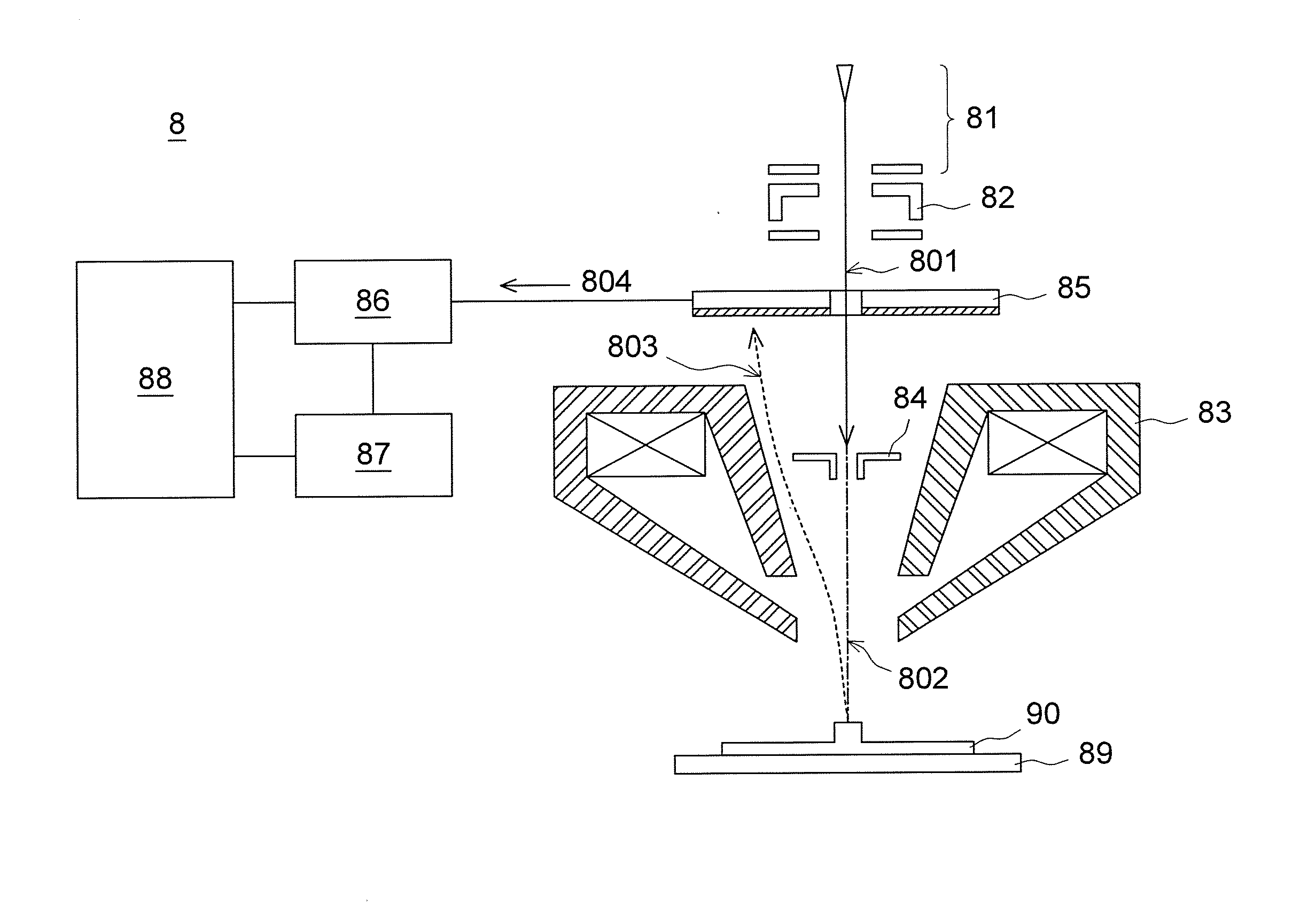
[0025]The specimen hereafter described will be referred to wafer or reticle, wherein the reticle is used in lithography. Wafer may include silicon wafer, silicon-germanium wafer, SOI wafer, or III-V or II-VI compound semiconductor wafer. This invention can be also applied to reticle inspection, especially EUV mask inspection.

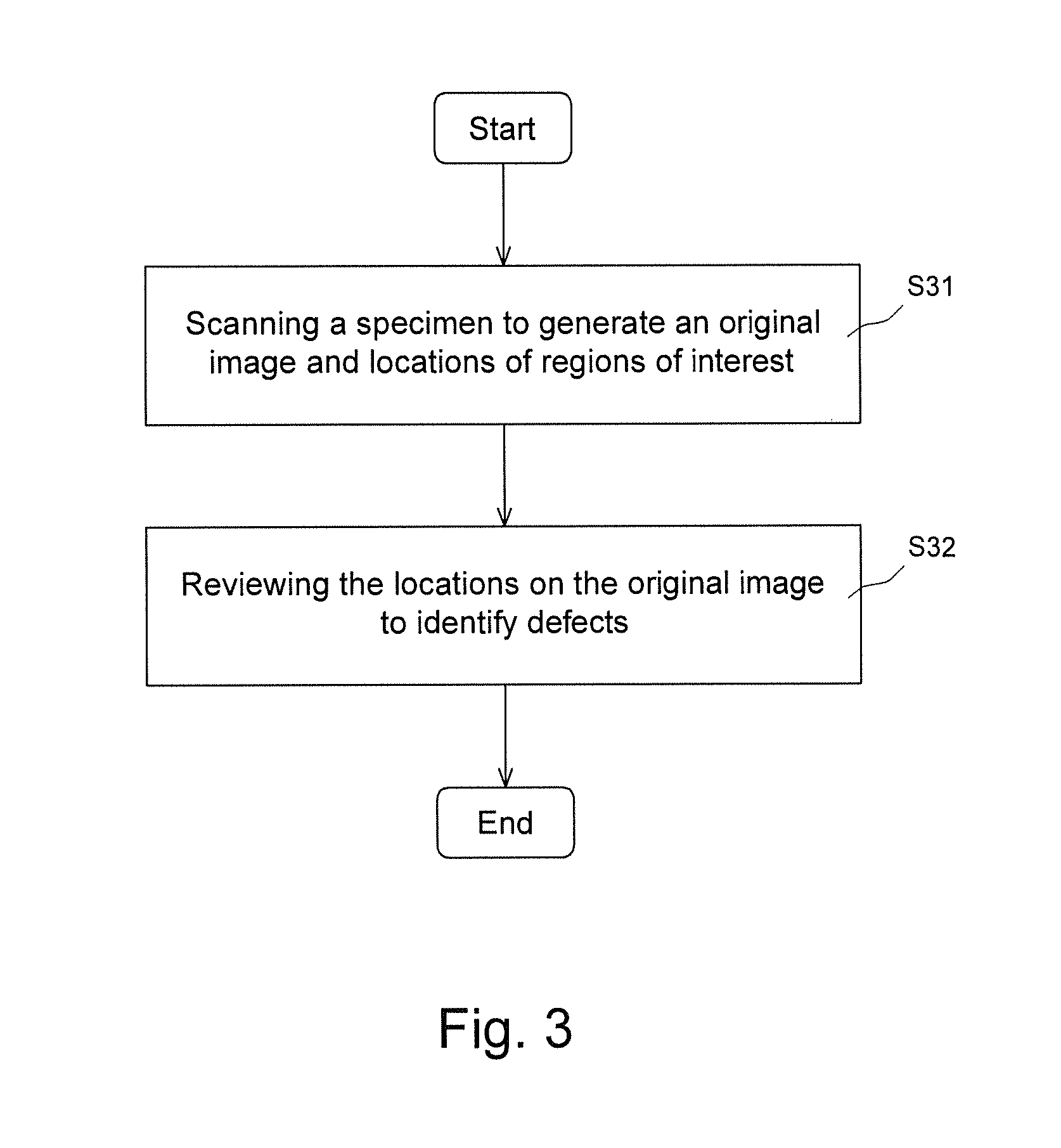
[0026]Referring to FIG. 3, a method for fast identifying defects according to an embodiment of the present invention includes scanning a specimen to generate an original image and locations of regions of interest (S31) and reviewing the locations on the original image to identify defects (S32). In one embodiment, the scanning step is processed by using an E-beam inspection tool or an optical inspection tool. Also refer...


PUM

PropertyMeasurementUnit
defectaaaaaaaaaa
Defect inspectionaaaaaaaaaa
SEMaaaaaaaaaa

Abstract

A method and system for inspecting defects saves scanned raw data as an original image so as to save time for repeated scanning and achieve faster defect inspection and lower false rate by reviewing suspicious defects and other regions of interest in the original image by using the same or different image-processing algorithm with the same or different parameters.

Description

RELATED APPLICATION[0001]This application is a Continuation Application of U.S. application Ser. No. 13 / 154,483, filed on Jun. 7, 2011, the entire contents of which are incorporated herein by reference.BACKGROUND OF THE INVENTION[0002]Field of the Invention[0003]The present invention relates to a method and system for inspecting defects, and more particularly to a method and system for fast inspecting defects which decreases false rate of defect inspection.[0004]Description of the Prior Art[0005]Defect inspection in the semiconductor device has always been one of important issues in semiconductor manufacturing process. Referring to FIG. 1, a conventional method for inspecting defects is achieved by obtaining a scanned image, e.g. an SEM (scanning electron microscope) image of a specimen such as a semiconductor device (S11) and identifying defects on the surface of the specimen within the scanned image (S12). Since the scanned data is of extremely enormous data volume and often large...

Claims


Application Information

Patent Timeline
Patent Type & Authority Patents(United States)
IPC IPC(8): G03F1/84G01N23/225H05K1/00G03F1/00G06T7/00G01N21/956
CPCG06T7/0004G01N23/2251G03F1/84G03F1/144H05K1/00G06T2207/30148G01N21/95607G06T2207/30141G03F1/86G03F7/7065G01N21/9501G06T2207/10061G06T7/001G03F1/36G06T7/0008H01J37/222H01J2237/2448H01J2237/2806
Inventor FANG, WEIJAU, JACK
Owner ASML NETHERLANDS BV
Why Eureka
Try Eureka