

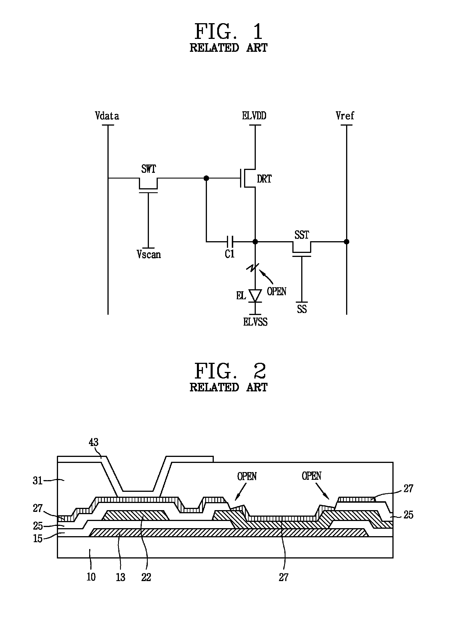
Organic light emitting diode display, and fabricating and inspecting methods thereof
a light-emitting diode and organic technology, applied in the direction of individual semiconductor device testing, transistors, solid-state devices, etc., can solve the problems of high probability of high-resolution display, failure of the line connecting the source electrode of the driving thin-film transistor drt and the anode electrode of the organic light-emitting diode el, corrosion, non-patterning or step difference failure, etc., to achieve the effect of reducing, through redund
- Summary
- Abstract
- Description
- Claims
- Application Information
AI Technical Summary
Benefits of technology
Problems solved by technology
Method used
Image

Examples
Embodiment Construction
[0032]Description will now be given in detail of the exemplary embodiments of the present invention, with reference to the accompanying drawings. For the sake of brief description with reference to the drawings, the same or equivalent components will be provided with the same reference numbers, and description thereof will not be repeated.
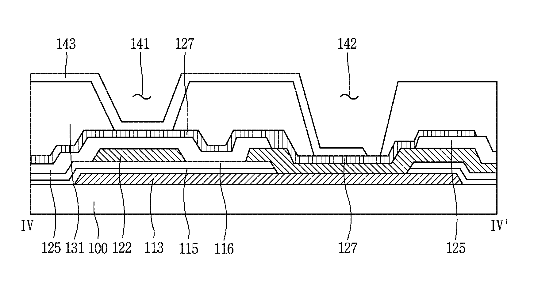
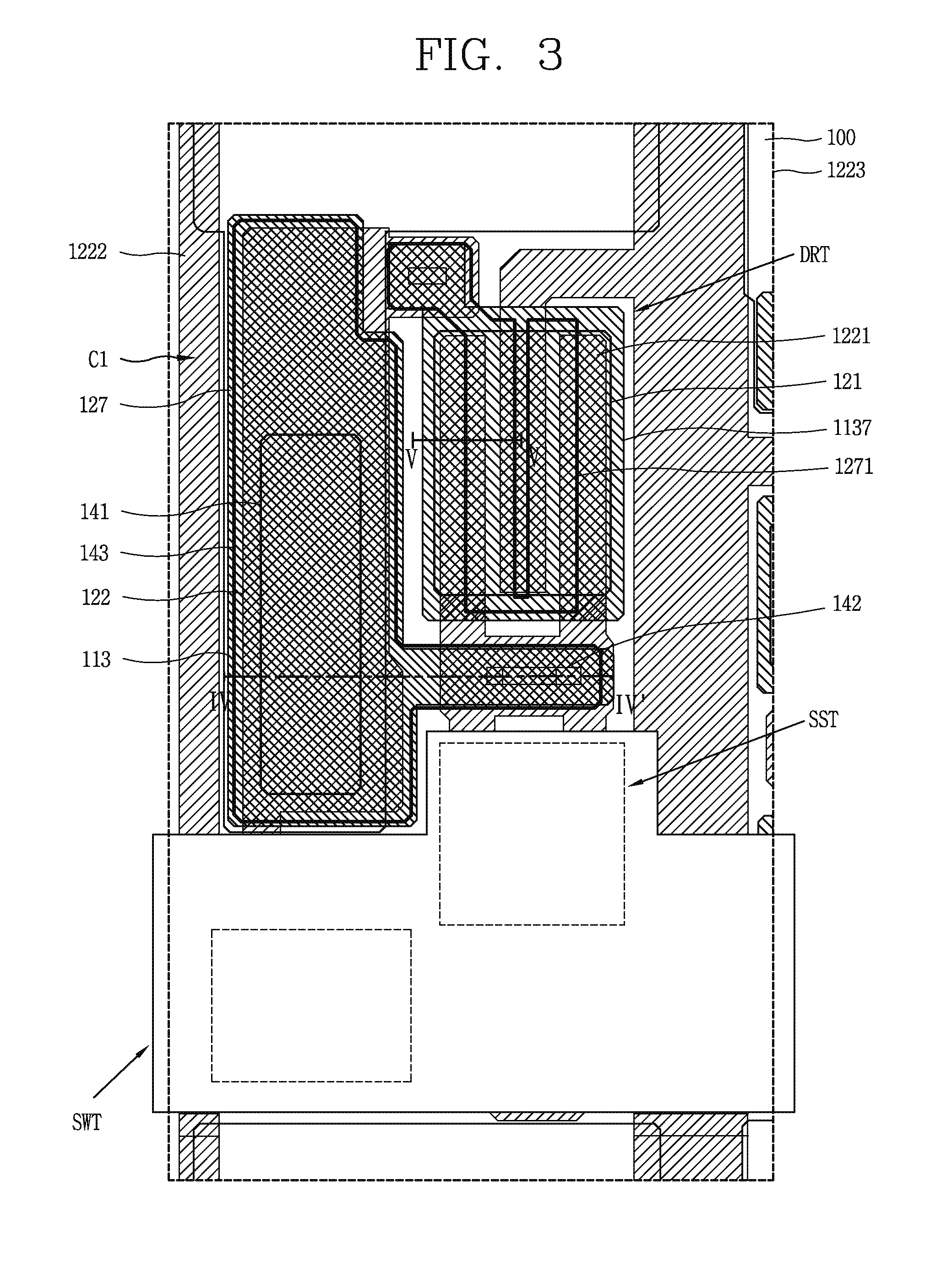
[0033]FIG. 3 is a plan view of a pixel of an organic light emitting diode display according to an exemplary embodiment of the present invention, and FIGS. 4A and 4B are section views respectively illustrating portions IV-IV′ and V-V′ of FIG. 3. The pixel of the organic light emitting diode display according to one or more embodiments of the present invention includes three thin film transistors.
[0034]Referring to FIGS. 3-4B, in the organic light emitting diode display according to the present disclosure, a gate metal layer 113 including a gate electrode and a signal line is formed on a substrate 100. Here, the substrate 100 may be made of a flexibl...
PUM
 Abstract
Description
Claims
Application Information