Low energy electron beam lithography

a low-energy, electron beam technology, applied in the direction of optics, photomechanical equipment, instruments, etc., can solve the problems of complex and expensive euv lithography system, not sure whether or not the system has been widely used, and achieve the effect of minimizing the placement error of the pattern

Inactive Publication Date: 2017-01-31
UTSUMI TAKAO
View PDF44 Cites 1 Cited by
  • Summary
  • Abstract
  • Description
  • Claims
  • Application Information

AI Technical Summary

Benefits of technology

[0021]The present invention relates to a system for integrated circuits to be mass-produced, for patterning an object having a characteristic whose minimum size is in the range of about 10 nm to 20 nm, and for low-energy electron beam lithography with sufficient throughputs and accuracy.
[0023]The present invention further comprises a matching detection unit and an inclination means. The matching detection unit detects a misalignment between the integrated mask wafer and semiconductor wafer. The inclination means has an input connected to an output of the matching detection unit in order to generate a correction signal in its output, which is then connected to an input of the micro deflection unit in order to compensate for a misalignment between the mask wafer and the semiconductor wafer and minimize a placement error of the pattern.
[0034]A step of detecting a misalignment between the mask wafer and the semiconductor wafer and generating a misalignment correction signal; and a step of applying the correction signal to the micro deflection unit for adjusting the inclination of the electron beams in order to compensate for the misalignment between the mask wafer and the semiconductor wafer and minimize a placement error of the pattern.

Problems solved by technology

Proposed systems such as the ArF double patterning and the EUV lithography system are complicated and expensive, and supposing those systems have been implemented, it is not sure whether or not those systems have widely been used.

Method used


Image

  • Low energy electron beam lithography
  • Low energy electron beam lithography
  • Low energy electron beam lithography

Examples


Embodiment Construction

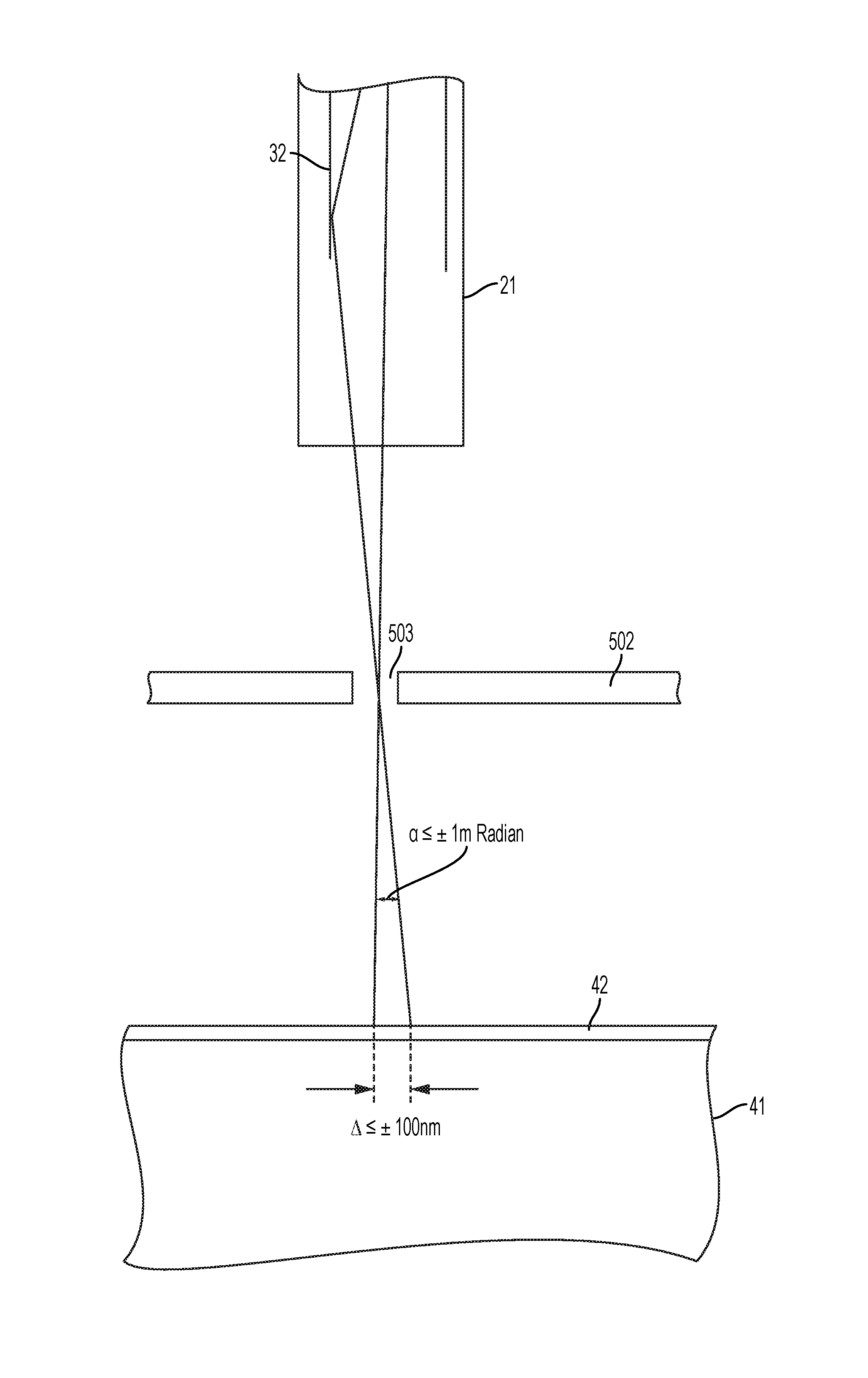
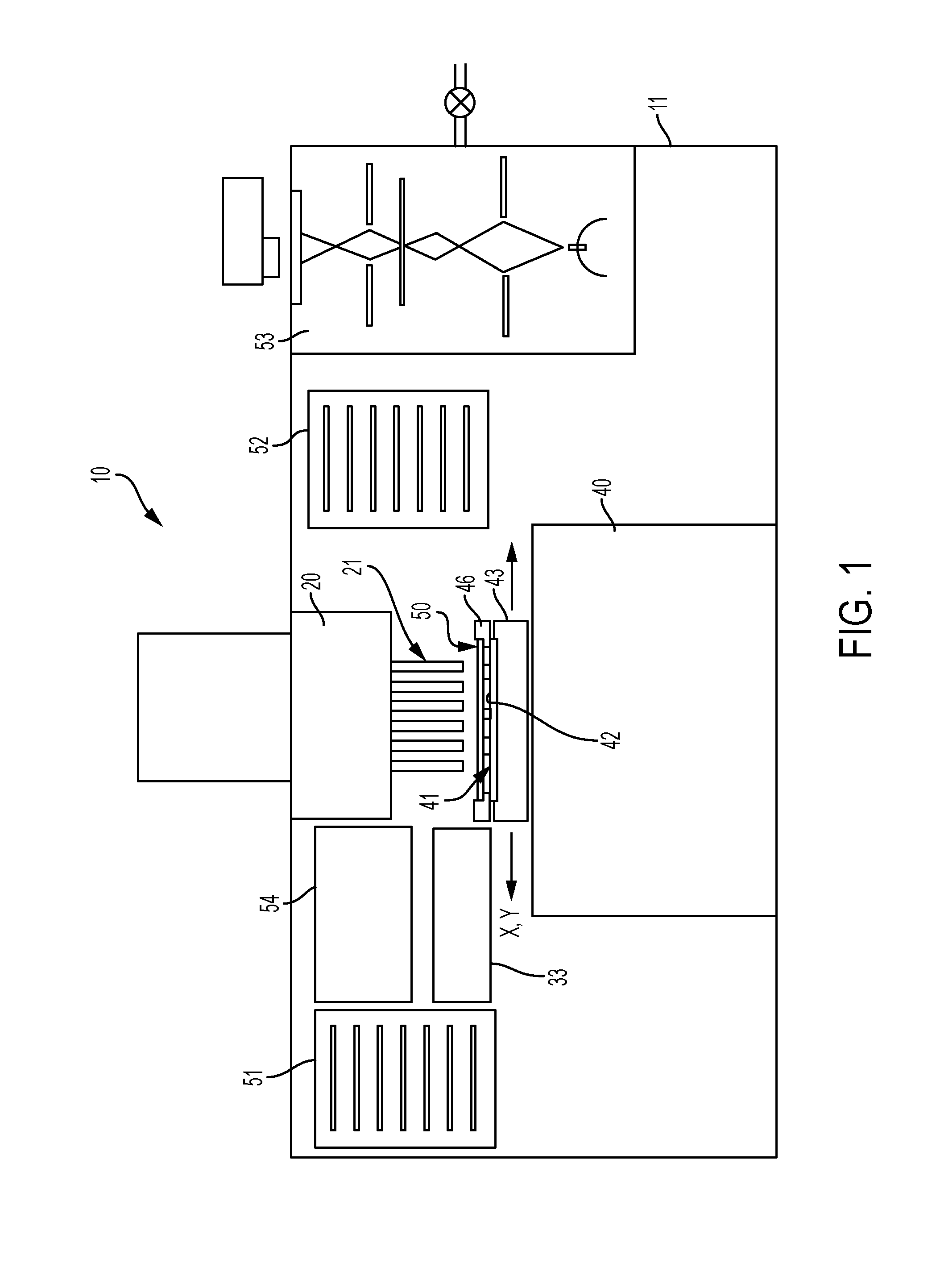
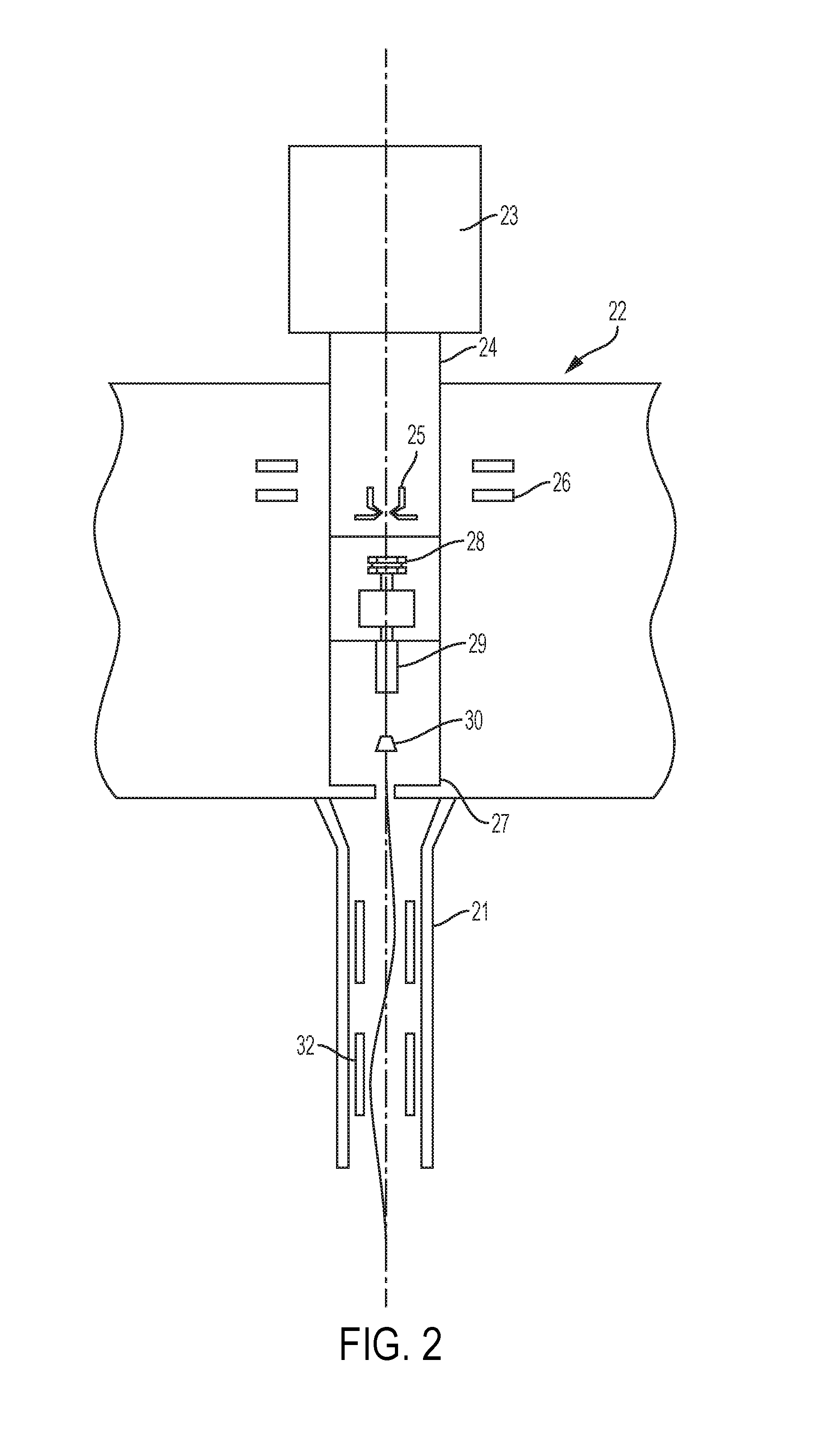
[0047]FIG. 1 shows a system (electron beam device) 10 according to the present invention. The system 10 has a casing 11, which contains the entire device and is provided with constituent elements as explained below inside. At the upper center section, an electron gun housing unit 20 is disposed. Within the electron gun housing unit 20, a plurality of electron guns is disposed in parallel with each other. FIG. 1 shows a hollow column 21 extending downward from each electron gun. In FIG. 1, only six columns extend due to the limitations of drawing, but a larger number of columns (and also electron guns) may be provided. Preferably, 10 columns (therefore 10 electron guns) are provided.

[0048]Within the housing 11 are disposed a movable stage 40, which can be moved in the X-Y directions, below the electron gun housing unit 20, a wafer stage 43 that is disposed on the movable stage and holds a semiconductor wafer 41, and a mask stage 46 that peripherally holds the mask wafer (stencil mask...


PUM

PropertyMeasurementUnit
diameteraaaaaaaaaa
thicknessaaaaaaaaaa
thicknessaaaaaaaaaa

Abstract

The system for drawing a pattern on a resist layer covering a semiconductor wafer, comprising an electron gun housing unit provided with a plurality of small-sized electron guns (wherein the housing unit has a hollow column section for releasing an electron beam, and a micro deflection unit is disposed inside for adjusting the inclination of the electron beam), a movable stage capable of moving in the X-Y directions, a wafer stage disposed on the movable stage to support a semiconductor wafer, a mask wafer having struts on its rear side for supporting membranes on which a pattern to be transferred is formed, a mask stage for holding the mask wafer, a matching detection unit for detecting a misalignment between the mask wafer and the semiconductor wafer, and an inclination means connected to the micro deflection unit and the matching detection unit for inclining the electron beam.

Description

FIELD OF THE INVENTION[0001]The present invention relates to the production of an integrated circuit device in which the size of an object having a minimum characteristics is about 10 nm to 20 nm, and particularly to a device and a method used for such a production.BACKGROUND OF THE INVENTION[0002]An important portion of the production of integrated circuits is patterning on the surface of a semiconductor wafer (which is cut into small pieces after processing to make integrated circuit devices). Such patterning defines various regions within an integrated circuit device including ion implantation regions, contact window regions and bonding pad regions, and is generally formed by transferring a geometrical shape pattern of a mask to a thin layer of a photosensitive material (which is called a “resist”) covering a silicon wafer, which forms an integrated circuit device. The pattern of a mask is typically enlarged, and therefore it needs to be reduced for the purpose of projection to a...

Claims


Application Information

Patent Timeline
Patent Type & Authority Patents(United States)
IPC IPC(8): H01J37/147H01L21/68H01L21/3065H01L21/308G03F7/20H01J37/04
CPCG03F7/70725H01L21/308H01L21/3065H01L21/681H01L21/682H01J37/09H01J37/3177H01J2237/0453H01J2237/1501
Inventor UTSUMI, TAKAO
Owner UTSUMI TAKAO
Why Eureka
Try Eureka