Subwavelength photonic crystal waveguide with trapezoidal shaped dielectric pillars in optical systems

a dielectric pillar and optical system technology, applied in the field of optical communication, biological sensing, chemical sensing, etc., can solve the problems of less attractive sensing platform for silicon, large challenge in generating or controlling photons, and increased radiation loss, so as to reduce the loss of bend, increase the loss, and reduce the effect of radiation loss

Active Publication Date: 2017-02-07
OMEGA OPTICS
View PDF2 Cites 7 Cited by
  • Summary
  • Abstract
  • Description
  • Claims
  • Application Information

AI Technical Summary

Benefits of technology

[0009]A trapezoidal shaped dielectric pillar based subwavelength photonic crystal waveguide bend is proposed herein, that is unique in that it provides the freedom to control the refractive index profile across the cross-section of a waveguide and therefore reduce the bend loss of a subwavelength photonic crystal waveguide. Compared to a straight waveguide, waveguide bends usually have additional loss due to the mode delocalization. The delocalized mode causes the mode mismatch between the straight and bend waveguide and hence excessive radiation loss. The mode delocalization is not prominent when the refractive index contrast between the waveguide core and cladding (e.g. silicon) is large and the bend radius is large. As an example, the insertion loss of a silicon strip waveguide bend can be ignored when its radius is larger than 1 μm. The equivalent refractive index of the subwavelength photonic crystal waveguide is relatively small so that the bending loss cannot be ignored. With the trapezoidal shaped dielectric pillars, the equivalent refractive index along the radial direction can be controlled to shift the mode back to the center of the subwavelength photonic crystal waveguide.

Problems solved by technology

However, the fact that silicon does not have either a direct band gap or a second-order nonlinearity makes it a great challenge to generate or control photons.
Additionally, the large refractive index contrast weakens the photon-matter interaction and makes silicon a less attractive sensing platform.
One critical problem remaining unresolved is the large loss of the subwavelength photonic crystal waveguide bends.
Although the strip waveguide bends can significantly reduce the loss, the taper adds additional loss and wastes the precious silicon chip surface.
Compared to a straight waveguide, waveguide bends usually have additional loss due to the mode delocalization.
The delocalized mode causes the mode mismatch between the straight and bend waveguide and hence excessive radiation loss.

Method used


Image

  • Subwavelength photonic crystal waveguide with trapezoidal shaped dielectric pillars in optical systems
  • Subwavelength photonic crystal waveguide with trapezoidal shaped dielectric pillars in optical systems
  • Subwavelength photonic crystal waveguide with trapezoidal shaped dielectric pillars in optical systems

Examples


Embodiment Construction

Detailed Description of the Invention

[0024]Detailed descriptions of the preferred embodiments are provided herein. It is to be understood, however, that the present invention may be embodied in various forms. The specific details disclosed herein are not to be interpreted as limiting, but rather as a basis for the claims and as representative basis for teaching one skilled in the art to employ the present invention in virtually any appropriately detailed system, structure, or manner. In all the accompanying drawings, same numerals are used within each figure to represent the same or similar materials, and redundant descriptions are omitted.

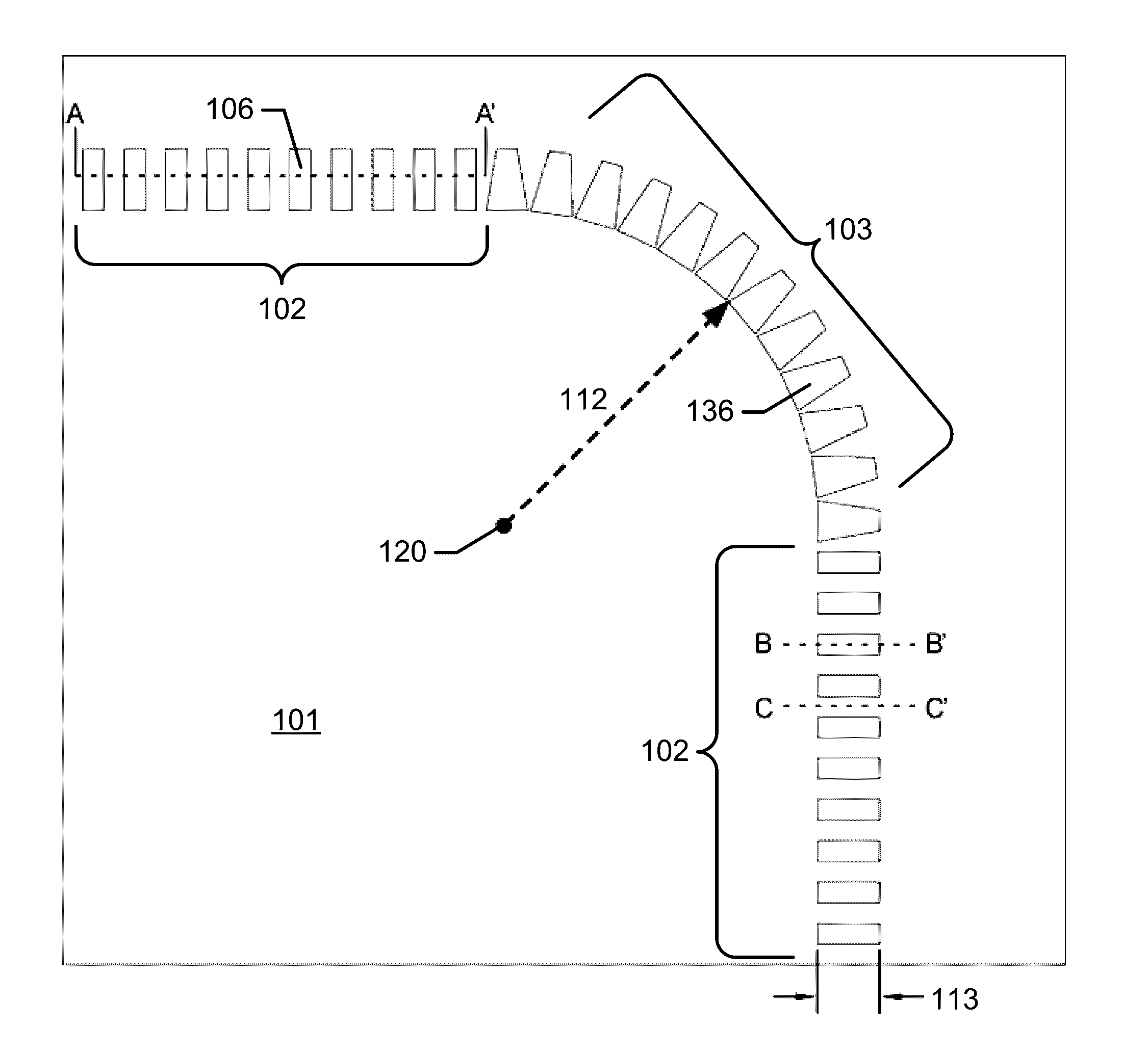
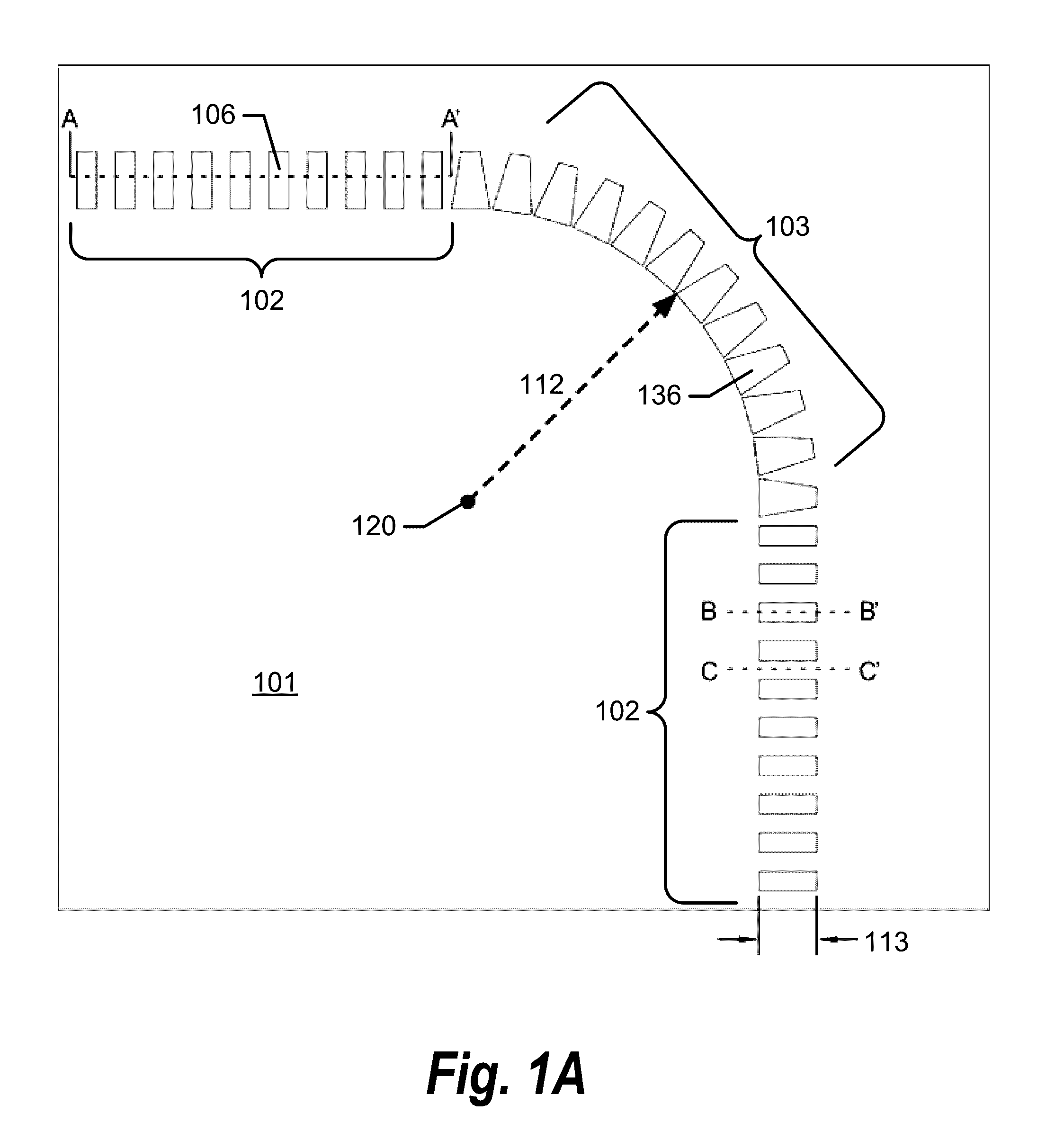
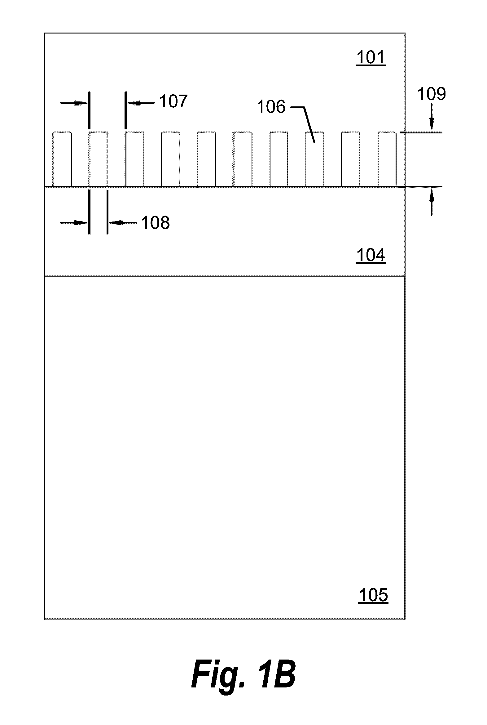
[0025]The invention discloses methods of reducing the loss of subwavelength photonic crystal waveguide bends and high quality factor subwavelength ring resonator based filters, modulators, and sensors. The low loss subwavelength photonic crystal waveguide bends are achieved by optimizing the shape of the dielectric pillars constituting the subwave...


PUM

PropertyMeasurementUnit
insertion lossaaaaaaaaaa
radiusaaaaaaaaaa
gap sizesaaaaaaaaaa

Abstract

A method for reducing loss in a subwavelength photonic crystal waveguide bend is disclosed. The method comprising: forming the subwavelength photonic crystal waveguide bend with a series of trapezoidal shaped dielectric pillars centered about a bend radius; wherein each of the trapezoidal shaped dielectric pillars comprise a top width, a bottom width, and a trapezoid height; wherein the length of the bottom width is greater than the length of the top width; and wherein the bottom width is closer to the center of the bend radius of the subwavelength photonic crystal waveguide bend than the top width. Other embodiments are described and claimed.

Description

I. STATEMENT REGARDING FEDERALLY SPONSORED RESEARCH[0001]This invention was made with Government support under grant DE-SC0013178 awarded by the Department of Energy (DOE). The Government has certain rights in this invention.II. BACKGROUND[0002]Field of the Invention[0003]The present disclosure relates generally to the field of optical and medical devices, and more specifically to an apparatus and method for optical communication, biological sensing, and chemical sensing.[0004]Background of the Invention[0005]The statements in this section merely provide background information related to the present disclosure and may not constitute prior art.[0006]Silicon photonics has been attracting intense interest in the last decade due to its great potential in realizing low cost photonic chips with the readily-available CMOS manufacture technology. However, the fact that silicon does not have either a direct band gap or a second-order nonlinearity makes it a great challenge to generate or con...

Claims


Application Information

Patent Timeline
Patent Type & Authority Patents(United States)
IPC IPC(8): G02F1/01G02B6/125G02B6/122G02B6/10G02B6/293G02F1/365G02B6/34
CPCG02B6/125G02B6/1225G02B6/107G02B6/29338G02B6/1228G02F1/365G02B6/34G02B6/29395G02F1/0147G02B6/12007G01N21/77G01N2021/7789
Inventor XU, XIAOCHUANCHEN, RAY T.
Owner OMEGA OPTICS
Why Eureka
Try Eureka