Subwavelength Photonic Crystal Waveguide in Optical Systems

a crystal waveguide and optical system technology, applied in the field of optical communication, biological sensing, chemical sensing, etc., can solve the problems of long-lasting search for a suitable integration platform, high cost, and inability to meet the requirements of the application, and achieve the effect of reducing the loss of bend, excessive radiation loss, and additional loss

Active Publication Date: 2017-05-25
OMEGA OPTICS
View PDF3 Cites 13 Cited by
  • Summary
  • Abstract
  • Description
  • Claims
  • Application Information

AI Technical Summary

Benefits of technology

[0013]In one embodiment, a trapezoidal shaped dielectric pillar based subwavelength photonic crystal waveguide bend is disclosed herein, that is unique in that it provides the freedom to control the refractive index profile across the cross-section of a waveguide and therefore reduce the bend loss of a subwavelength photonic crystal waveguide. Compared to a straight waveguide, waveguide bends usually have additional loss due to the mode delocalization. The delocalized mode causes the mode mismatch between the straight and bend waveguide and hence excessive radiation loss. The mode delocalization is not prominent when the refractive index contrast between the waveguide core and cladding (e.g. silicon) is large and the bend radius is large. As an example, the insertion loss of a silicon strip waveguide bend can be ignored when its radius is larger than 1 μm. The equivalent refractive index of the subwavelength photonic crystal waveguide is relatively small so that the bending loss cannot be ignored. With the trapezoidal shaped dielectric pillars, the equivalent refractive index along the radial direction may be controlled to shift the mode back to the center of the subwavelength photonic crystal waveguide.
[0014]With the trapezoidal shaped subwavelength photonic crystal waveguide bend, the quality factor of the subwavelength ring resonator may be significantly improved. A typical optical system employing the high quality factor ring resonator may comprise: a substrate with a bottom cladding to support the structure, a light source, couplers to interface the light source and the optical circuits, tapers to convert the light from a conventional waveguide into a subwavelength photonic crystal waveguide, a ring resonator formed by a periodic arrangement of trapezoidal shaped dielectric pillars, and a subwavelength photonic crystal bus waveguide.

Problems solved by technology

Conventional photonic devices are bulky, heavy, expensive, and susceptible to environmental fluctuations, and it is widely accepted that integrated photonics is a promising alternative.
However, the search for a suitable integration platform turns out to be a long-lasting effort.
A number of material platforms have been explored, such as ion-exchanged glass, Indium Phosphide (InP), silicon-on-insulator (SOI), and polymer, but none of them is perfect.
However, the fact that silicon does not have either a direct band gap or a second-order nonlinearity makes it a great challenge to generate or control photons.
Additionally, the large refractive index contrast weakens the photon-matter interaction and makes silicon a less attractive sensing platform.
However, so far the research on subwavelength photonic crystal waveguide is limited to two materials, and the shape of these materials are usually circular or rectangular.
These unnecessary constraints greatly limit the applications of subwavelength photonic crystal waveguides.
For example, one critical problem remaining unresolved is the large loss of the subwavelength photonic crystal waveguide bends.
Although the strip waveguide bends can significantly reduce the loss, the taper adds additional loss and wastes the precious silicon chip surface.
Compared to a straight waveguide, waveguide bends usually have additional loss due to the mode delocalization.
The delocalized mode causes the mode mismatch between the straight and bend waveguide and hence excessive radiation loss.

Method used


Image

  • Subwavelength Photonic Crystal Waveguide in Optical Systems
  • Subwavelength Photonic Crystal Waveguide in Optical Systems
  • Subwavelength Photonic Crystal Waveguide in Optical Systems

Examples


Embodiment Construction

Detailed Description of the Invention

[0040]Detailed descriptions of the preferred embodiments are provided herein. It is to be understood, however, that the present invention may be embodied in various forms. The specific details disclosed herein are not to be interpreted as limiting, but rather as a basis for the claims and as representative basis for teaching one skilled in the art to employ the present invention in virtually any appropriately detailed system, structure, or manner. In all the accompanying drawings, same numerals are used within each figure to represent the same or similar materials, and redundant descriptions are omitted.

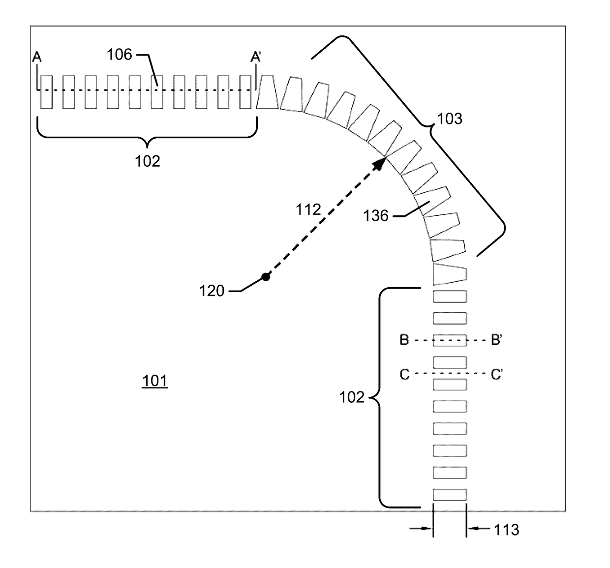
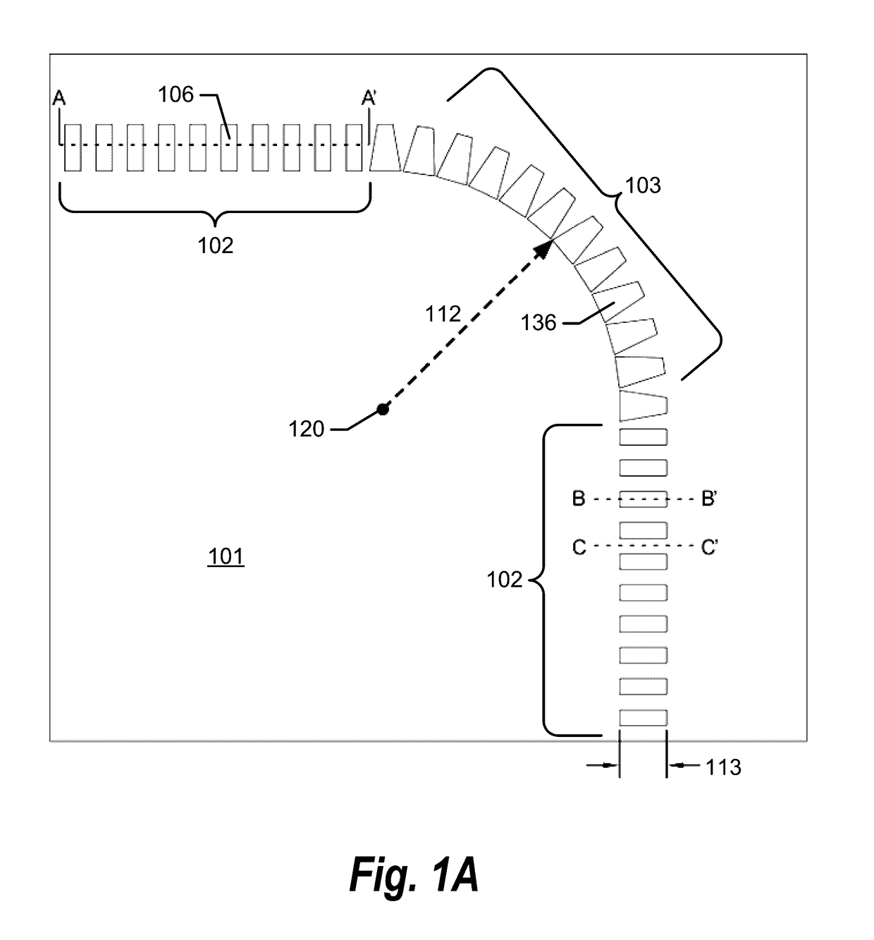
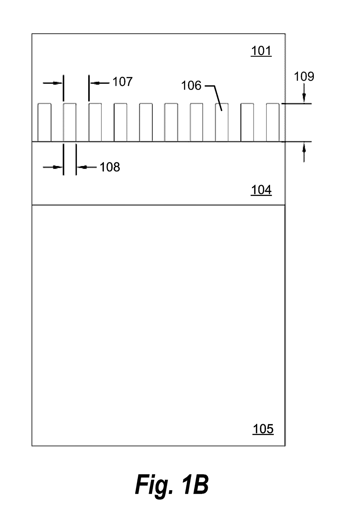
[0041]The invention discloses methods of reducing the loss of subwavelength photonic crystal waveguide bends and high quality factor subwavelength ring resonator based filters, modulators, and sensors. The low loss subwavelength photonic crystal waveguide bends are achieved by optimizing the shape of the dielectric pillars comprising the subwavele...


PUM


Abstract

An optical system is disclosed. The optical system comprising: a substrate; and a subwavelength photonic crystal waveguide atop the substrate, wherein the subwavelength photonic crystal waveguide comprises a periodic one or two-dimensional array of two or more interleaved dielectric pillars; wherein the periodicity of the one or two-dimensional array is constant, a combination of two or more periods, or random; wherein the one or two-dimensional array is substantially linear or curved; wherein each of the pillars of the one or two-dimensional array is at least one of a triangular prism, a trapezoidal prism, an elliptic cylinder, a cylinder, a tube, a frustum, a pyramid, a trapezoidal prism, and an asymmetric frustum; and wherein each of the pillars of the one or two-dimensional array comprises a solid, liquid, and/or gas. Other embodiments are described and claimed.

Description

CROSS REFERENCE TO RELATED APPLICATIONS[0001]The application is a continuation-in-part application of U.S. patent application Ser. No. 14 / 951,464, titled “Subwavelength Photonic Crystal Waveguide with Trapezoidal Shaped Dielectric Pillars in Optical Systems”, filed Nov. 24, 2015, the contents of which is all hereby incorporated by reference.STATEMENT REGARDING FEDERALLY SPONSORED RESEARCH[0002]This invention was made with Government support under grant DE-SC0013178 awarded by the Department of Energy (DOE). The Government has certain rights in this invention.BACKGROUND[0003]Field of the Invention[0004]The present disclosure relates generally to the field of optical and medical devices, and more specifically to an apparatus and method for optical communication, biological sensing, and chemical sensing.[0005]Background of the Invention[0006]The statements in this section merely provide background information related to the present disclosure and may not constitute prior art.[0007]Inte...

Claims


Application Information

Patent Timeline
Patent Type & Authority Applications(United States)
IPC IPC(8): G02B6/122G02B6/125G02B6/10
CPCG02B6/1225G02B6/125G02B6/107G02B6/12007G02B6/1228G02B6/29338G02B6/29395G02B6/34G02F1/0147G02F1/365
Inventor XU, XIAOCHUANCHEN, RAY T.
Owner OMEGA OPTICS
Why Eureka
Try Eureka