
Electro-optic device, method of manufacturing electro-optic device, and electronic apparatus

a manufacturing method and electrooptic technology, applied in the direction of organic semiconductor devices, solid-state devices, discharge tubes luminescnet screens, etc., can solve the problems of light emission regions, light-emitting elements, and increase in size in the entire region of the element substrate, so as to prevent curvature, distortion, or small differences between the related refractive index

Active Publication Date: 2017-03-21
SEIKO EPSON CORP
View PDF16 Cites 6 Cited by
  • Summary
  • Abstract
  • Description
  • Claims
  • Application Information

AI Technical Summary

Benefits of technology

This configuration effectively minimizes the frame region, reduces resin material variation, and prevents bubble formation between resin layers, enhancing the reliability and light transmission efficiency of the electro-optic device.

Problems solved by technology

In the electro-optic device disclosed in JP-A-2008-59868, however, since the sealing member is disposed on the outside of the region in which the light-emitting elements are disposed, there is a problem that a region (so-called frame region) on the outside of the region (light emission region) in which the light-emitting elements are disposed increases in size in the entire region on the element substrate.
Also, there is a problem that the resin material filling the inside of the sealing member protrudes to the outside of the sealing member when one substrate is pressed against the other substrate, or curving or distortion occurs in the element substrate or the counter substrate since the thickness of the sealing member and the thickness of the resin material become non-uniform due to contraction (volume variation) when the resin material is hardened.
However, when the resin material has low viscosity, wet-spreading occurs up to a range more than necessary before the applied resin material is hardened, and thus for example, there is a problem that a defect such as overlapping of the resin material with a terminal section may occur.
However, since the low-viscosity resin material is used in the first resin layer covering at least the light-emitting elements, there is a problem that it is difficult to remove the wet-spreading of the resin material when the first resin layer is formed.
Also, since a difference occurs in the degree of the wet-spreading of the resin material depending on an elapsed time after the application of the resin material, there is also a problem that a variation occurs between individual devices.
Then, there is a problem that pressure applied between the substrates may not be uniform, bubbles may be generated between the first resin layer and the second resin layer, or a variation may occur in the wet-spreading of the second resin layer when the mother substrate is adhered to the counter substrate by the second resin layer.

Method used


Image

  • Electro-optic device, method of manufacturing electro-optic device, and electronic apparatus
  • Electro-optic device, method of manufacturing electro-optic device, and electronic apparatus
  • Electro-optic device, method of manufacturing electro-optic device, and electronic apparatus

Examples


first embodiment

Organic EL Device

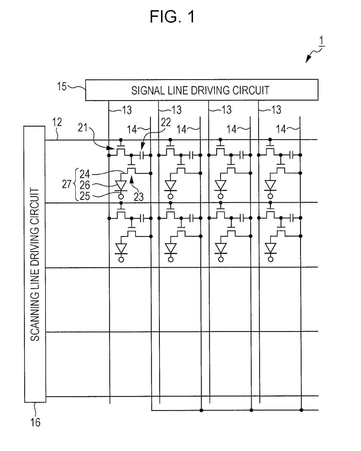
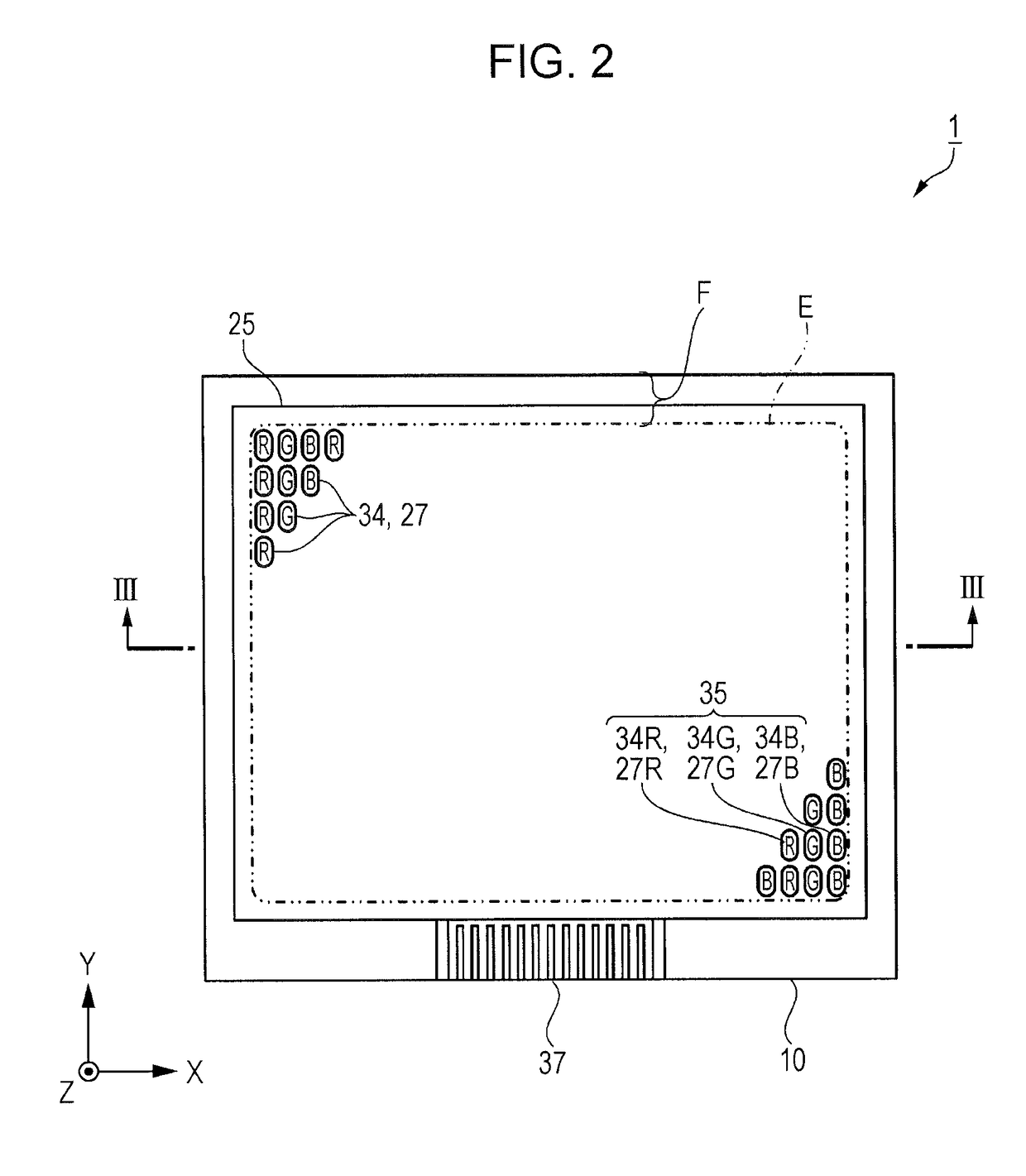
[0059]First, the configuration of an organic EL device which is an electro-optic device according to a first embodiment will be described with reference to the drawings. FIG. 1 is an equivalent circuit diagram illustrating an electric configuration of the organic EL device according to the first embodiment. FIG. 2 is a schematic plan view illustrating the configuration of the organic EL device according to the first embodiment. In FIG. 2, a counter substrate 48 (see FIG. 3) is not illustrated.

[0060]As illustrated in FIG. 1, an organic EL device 1 is an active matrix type organic EL device in which transistors are used as switching elements. The transistor is, for example, a thin film transistor (hereinafter referred to as a TFT) using a thin film semiconductor layer.

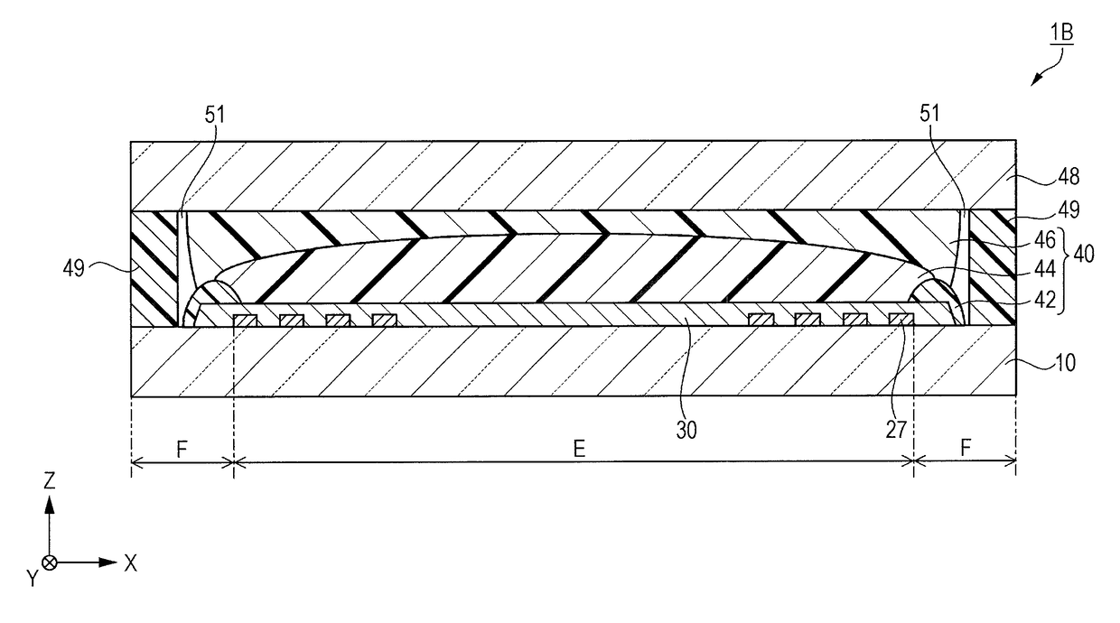
[0061]The organic EL device 1 includes an element substrate 10 (see FIG. 2) which is a first substrate, scanning lines 12 that are installed on a first surface 10a (see FIG. 3) of the element substrate 1...

second embodiment

Electro-Optic Device

[0156]Next, a light-receiving and emitting device which is an electro-optic device according to a second embodiment will be described with reference to FIG. 10. FIG. 10 is a schematic sectional view illustrating the configuration of an organic EL device according to the second embodiment. As illustrated in FIG. 10, a light-receiving and emitting device 3 according to the second embodiment is an electro-optic device configured by combining an organic EL device 1A which is an electro-optic device and a light-receiving device 2 which is an electro-optic device.

[0157]First, the organic EL device 1A will be described. The organic EL device 1A is disposed on a counter substrate 85 of the light-receiving device 2. The organic EL device 1A is different from the organic EL device 1 according to the first embodiment in that micro-lenses 47 are formed on the surface 48a of the counter substrate 48 and is the same as the organic EL device 1 in the remaining configuration. Th...

third embodiment

Electronic Apparatus

[0174]Next, an electronic apparatus according to a third embodiment will be described with reference to FIG. 11. FIG. 11 is a schematic diagram illustrating the configuration of a head-mounted display which is an electronic apparatus according to a third embodiment.

[0175]As illustrated in FIG. 11, a head-mounted display (HMD) 100 according to the third embodiment includes two display units 101 installed to correspond to left and right eyes. A viewer M can view text, images, or the like displayed on the display units 101 when the viewer M mounts the head-mounted display 100 on his or her head part like glasses. For example, when images in consideration of parallax are displayed on the left and right display units 101, the viewer M can view and enjoy a stereoscopic image.

[0176]The organic EL device 1 according to the first embodiment is mounted on each display unit 101. Accordingly, it is possible to provide the head-mounted display 100 that has excellent display q...


PUM


Abstract

An electro-optic device includes: a first substrate that includes a first surface; an optical element that is disposed in a first region on the first surface; a casing that is disposed to overlap with a part of the optical element along an outer periphery of the first region on the first surface and includes first and second end portions; a first resin layer that is disposed on an inside of the second end portion of the casing on the first surface and is installed to overlap with at least a part of the optical element; a second resin layer that is disposed on the first resin layer; and a second substrate that faces the first surface and is disposed on the second resin layer.

Description

BACKGROUND[0001]1. Technical Field[0002]The present invention relates to an electro-optic device, a method of manufacturing the electro-optic device, and an electronic apparatus.[0003]2. Related Art[0004]Electro-optic devices are known in which an element substrate in which optical elements such as light-emitting elements or light-receiving elements are disposed and a counter substrate facing to the surface of the element substrate on which the optical elements are disposed are bonded (for example, see JP-A-2008-59868). In the electro-optic device (organic EL device) disclosed in JP-A-2008-59868, an element substrate and a counter substrate (sealing substrate) are bonded via a sealing member disposed on the outside of a region in which light-emitting elements are disposed. The inside surrounded by the sealing member is filled with a resin material (filling layer) to alleviate stress, impact, or the like applied from the outside. Thus, it is possible to prevent the counter substrate ...

Claims


Application Information

Patent Timeline
Patent Type & Authority Patents(United States)
IPC IPC(8): H01L51/00H01L33/00H01J63/04H01J1/62H01L21/00H01L51/52H10K99/00
CPCH01L51/5246H01L51/524H01L51/5237H01L51/5253H01L2251/558H10K50/8426H10K2102/351H10K59/871H10K50/84H10K50/841H10K50/844
Inventor FUKAGAWA, TAKEFUMI
Owner SEIKO EPSON CORP
Learn More