Structure and method for diminishing delamination of packaged semiconductor devices

a semiconductor device and packaging technology, applied in semiconductor devices, semiconductor/solid-state device details, electrical devices, etc., can solve the problems of increasing complexity in material validation, device vulnerability, and time-consuming material validation, and achieve easy to use, facilitate adhesion, and enhance adhesion.

Active Publication Date: 2017-04-18
TEXAS INSTR INC
View PDF7 Cites 11 Cited by
  • Summary
  • Abstract
  • Description
  • Claims
  • Application Information

AI Technical Summary

Benefits of technology

[0007]Rather than solely focusing on enhancing adhesion between package and assembled device, applicant found a solution to drastically diminish delamination between package and assembled device, when he discovered a low-cost, readily available and flexible method of creating mechanical obstacles against delamination by extending and modifying the well-controlled wire bonding technology. Based on the strength of diffusion bonds, a plurality of mechanical anchor studs are created in quick sequence, which offer additional surface area to promote adhesion. Some studs may be arranged sequentially in the plane of the leadframe, others may be created as vertical stacks. The effectiveness of studs can be enhanced by adding wire arches spanned by the same wire bonding capillary forming the studs. The arches act as mold locks after curing the molding compound.

Problems solved by technology

Consequently, there is persistent pressure on the manufacturer to be the first one to offer a new product; he must try to shorten the product introduction and the time-to-market for a new product.
They employ a number of different materials, which make the devices vulnerable to the phenomenon of delamination between the package material and the encapsulated device.
Further, market pressure for product introduction makes time-consuming validation of materials and manufacturability ever more complicated.

Method used


Image

  • Structure and method for diminishing delamination of packaged semiconductor devices
  • Structure and method for diminishing delamination of packaged semiconductor devices
  • Structure and method for diminishing delamination of packaged semiconductor devices

Examples


Embodiment Construction

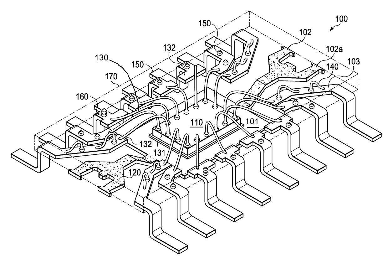
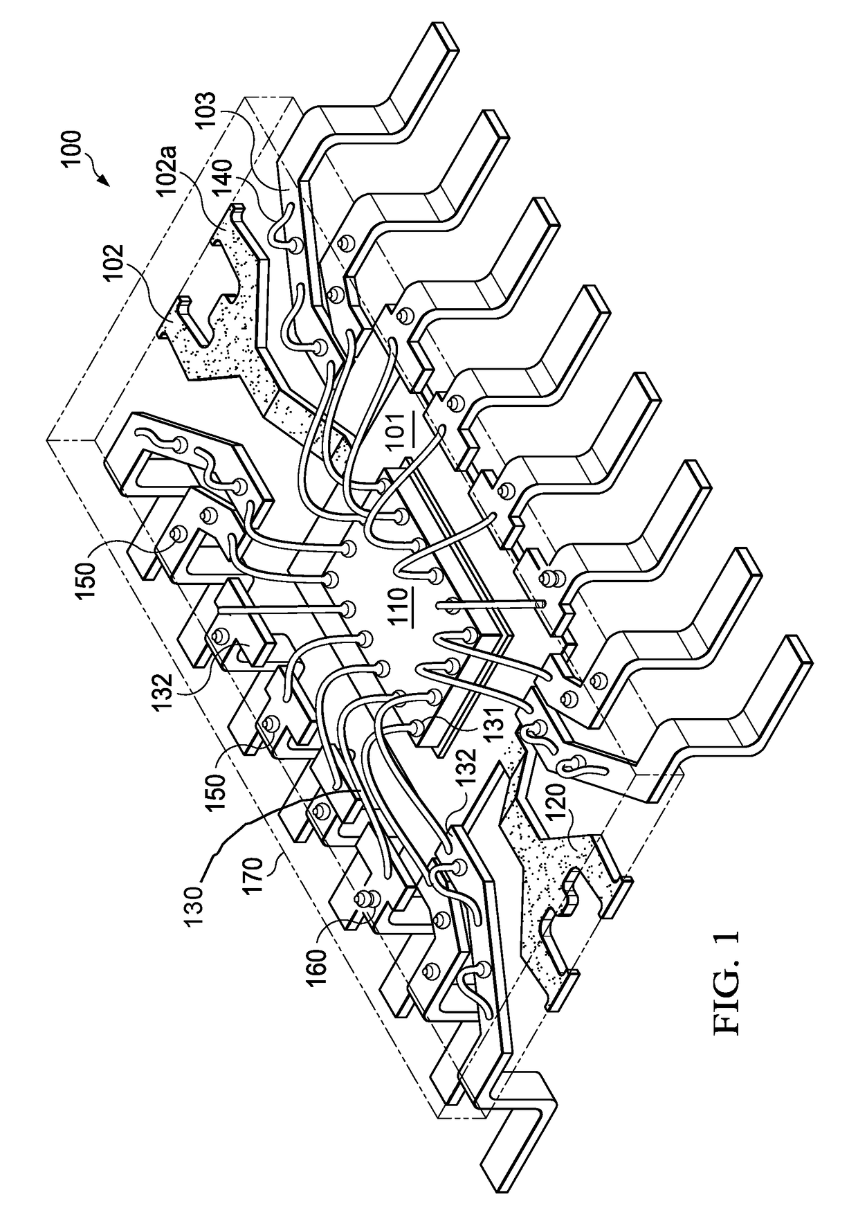
[0014]Embodiments of the invention are found in devices with semiconductor chips assembled on a support such as a metallic leadframe or a laminated substrate and encapsulated in a package of a polymeric compound. FIG. 1 illustrates an exemplary embodiment comprising a plastic packaged semiconductor device generally designated 100 with a substrate realized as a metallic leadframe. The leadframe includes a pad 101 for assembling a semiconductor chip 110, tie bars 102 connecting pad 101 to the sidewall of the package, and a plurality of leads 103. It should be noted that herein the tie bars are referred to as straps. The chip terminals are connected to the leads 103 by bonding wires 130, which include ball bond 131 and stitch bond 132. In the example of FIG. 1, leads 103 are shaped as cantilevered leads; in other embodiments, the leads may have the shape of flat leads as used in Quad Flat No-Lead (QFN) devices or in Small Outline No-Lead (SON) devices. Along their longitudinal extensio...


PUM


Abstract

A semiconductor device (100) comprising a leadframe with a pad (101) and elongated leads (103) made of a base metal plated with a layer enabling metal-to-metal bonding; a semiconductor chip (110) attached to the pad, the chip having terminals. A metallic wire connection (130) from a terminal to a respective lead, the connection including a first ball bond by a first squashed ball (131) attached to the terminal, and a first stitch bond (132) attached to the lead. A second squashed ball (150) of the wire metal attached to the lead as a second ball bond adjacent to the first stitch bond (132). A package (170) of a polymeric compound encapsulating the chip, wire connection, second ball and at least a portion of the elongated lead, the compound adhering to the materials of the encapsulated entities.

Description

FIELD[0001]Embodiments of the invention are related in general to the field of semiconductor devices and processes, and more specifically to the structure and fabrication method of assembled semiconductor devices with mechanical features for reducing the risk of delamination of packaged devices.DESCRIPTION OF RELATED ART[0002]Moisture-induced failures of plastic packaged semiconductor devices have been observed and investigated for many years. It is well known that plastic packages made, for instance, by epoxy-based molding compounds can be penetrated by discrete water molecules within a time period of about one day. However, this penetration does not lead to a problematic situation as long as there is good adhesion inside the package between the plastic compound and the device components (semiconductor chip, metallic leadframe, substrate, etc.), and the penetrated water molecules cannot accumulate to form films of water on free surfaces.[0003]In contrast, when some interfacial dela...

Claims


Application Information

Patent Timeline
Patent Type & Authority Patents(United States)
IPC IPC(8): H01L23/49H01L23/00H01L23/495H01L23/31H01L21/56H01L21/48
CPCH01L23/4952H01L24/46H01L23/3157H01L23/49582H01L23/49534H01L21/4853H01L21/56H01L2224/4945H01L2224/48091H01L2224/45124H01L2924/18301H01L24/49H01L2224/05624H01L23/3107H01L2224/45015H01L23/49551H01L2224/05647H01L24/48H01L2224/85045H01L2224/45144H01L24/45H01L2924/19107H01L2224/45147H01L2224/48465H01L24/05H01L23/49568H01L2924/00014H01L2924/20751H01L2924/20752H01L2924/20753
Inventor FLESSNER, KYLE MITCHELL
Owner TEXAS INSTR INC
Why Eureka
Try Eureka