Fin field effect transistor and method of manufacturing the same
a technology of field effect transistor and manufacturing method, which is applied in the direction of basic electric elements, semiconductor devices, electrical equipment, etc., can solve the problems of considering the electrical properties of devices, and achieve the effect of improving the electrical performance of fin
- Summary
- Abstract
- Description
- Claims
- Application Information
AI Technical Summary
Benefits of technology
Problems solved by technology
Method used
Image

Examples
first embodiment
[First Embodiment]
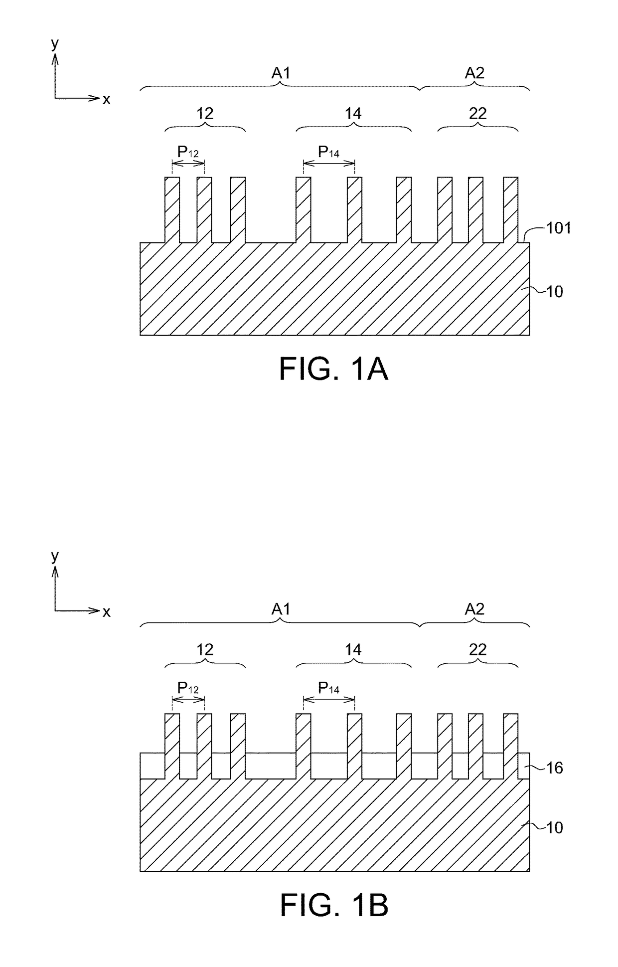
[0020]FIG. 1A˜FIG. 1G illustrate a method for manufacturing a FinFET according to the first embodiment of the present disclosure. First, a substrate 10 having a top surface 101 comprises a first area A1 with plural first protruding fins 12 and 14 and a second area A2 with plural second fins 22 are provided. As shown in FIG. 1A, the densely-distributed first protruding fins 12 and the loosely-distributed first protruding fins 14 are positioned in the first area A1, and the second fins 22 are positioned in the second area A2. The phrases of “densely-distributed” and “loosely-distributed” can be defined according to the pitches of the fins. In the embodiment, a pitch P12 of the densely-distributed first protruding fins 12 is smaller than a pitch P14 of the loosely-distributed first protruding fins 14.
[0021]As shown in FIG. 1B, an insulating layer 16 is formed on the top surface 101 of the substrate 10 for isolating the first protruding fins (i.e. densely-distributed f...
second embodiment
[Second Embodiment]
[0034]FIG. 2A˜FIG. 2F illustrate a method for manufacturing a FinFET according to the second embodiment of the present disclosure. Steps of the second embodiment are similar to that of the first embodiment, except for the changing of the order of steps. The identical elements of the first and second embodiments are designated with the same reference numerals. It is noted that steps as depicted in FIG. 2A˜FIG. 2C are identical to steps illustrated in FIG. 1A˜FIG. 1C, FIG. 6 and FIG. 7. Please refer to the first embodiment for the descriptions of the related elements, and the details are not redundantly repeated.
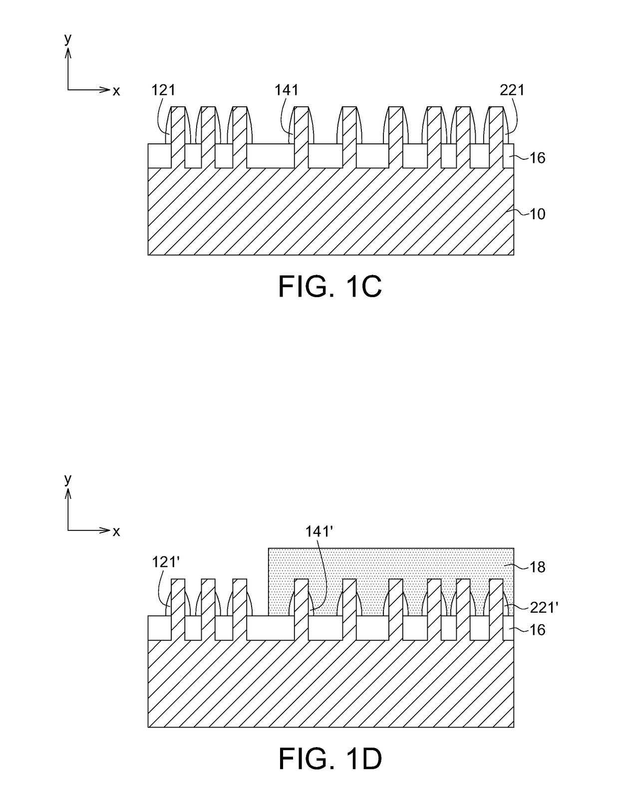
[0035]In the second embodiment, no shrinking step is performed on the spacers. Also, the mask layer 18 can be removed before removing the spacers.
[0036]As shown in FIG. 2D, a mask layer 18 is provided for shielding the predetermined portions after forming the spacers (i.e. the first spacers 121 and 141 respectively on the sidewalls of the densely-distributed...
third embodiment
[Third Embodiment]
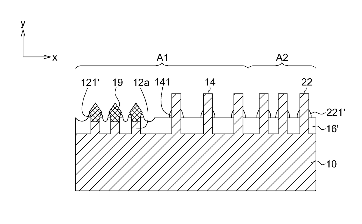
[0039]FIG. 3 illustrates a FinFET manufactured according to the third embodiment of the present disclosure. In the third embodiment, the spacers short in height can be kept on the insulation 16′ (ex: the lateral portions 16L of the first insulating regions 16-1) when the Epi layers 19 are grown. Manufacturing steps of the third embodiment can be referred to that of the first embodiment, and the details are not redundantly repeated. Identical elements of the third and the first embodiments are designated with the same reference numerals.
[0040]In one embodiment, the spacers, including the first spacers 121′ and 141′ on the densely-distributed first protruding fins 12 and the loosely-distributed first protruding fins 14 and the second spacers 221′ on the second fins 22, can be kept on the insulation 16′ if a height of the spacers is no more than 5 nm.
[0041]In an alternated embodiment, the spacers (including the first spacers 121′ and 141′ on the densely-distributed fi...
PUM
 Abstract
Description
Claims
Application Information
 - R&D
- Intellectual Property
- Life Sciences
- Materials
- Tech Scout
- Unparalleled Data Quality
- Higher Quality Content
- 60% Fewer Hallucinations
Browse by: Latest US Patents, China's latest patents, Technical Efficacy Thesaurus, Application Domain, Technology Topic, Popular Technical Reports.
© 2025 PatSnap. All rights reserved.Legal|Privacy policy|Modern Slavery Act Transparency Statement|Sitemap|About US| Contact US: help@patsnap.com