Semiconductor device, display device, input/output device, and electronic device

a technology of semiconductor devices and display devices, applied in the direction of semiconductor devices, electrical devices, transistors, etc., can solve the problems of difficult to obtain stable semiconductor characteristics and hydrogen diffusion into, and achieve excellent electrical characteristics, small variations in electrical characteristics, and high on-state current

Inactive Publication Date: 2017-04-25
SEMICON ENERGY LAB CO LTD
View PDF165 Cites 2 Cited by
  • Summary
  • Abstract
  • Description
  • Claims
  • Application Information

AI Technical Summary

Benefits of technology

[0010]In view of the above, an object of one embodiment of the present invention is to provide a self-aligned transistor including an oxide semiconductor film that has excellent electrical characteristics. Another object of one embodiment of the present invention is to provide a transistor having high on-state current. Another object of one embodiment of the present invention is to provide a method for manufacturing a transistor with small variations in electrical characteristics. Another object of one embodiment of the present invention is to provide a method for manufacturing a display device consuming less power. Another object of one embodiment of the present invention is to provide a novel method for manufacturing a display device.
[0020]One embodiment of the present invention can provide a self-aligned transistor including an oxide semiconductor film, which has excellent electrical characteristics. One embodiment of the present invention can provide a transistor having high on-state current. One embodiment of the present invention can provide a method for manufacturing a transistor with small variations in electrical characteristics. One embodiment of the present invention can provide a method for manufacturing a display device with low power consumption. One embodiment of the present invention can provide a novel method for manufacturing a display device.

Problems solved by technology

However, in this method, hydrogen might diffuse into the channel region and it is difficult to obtain stable semiconductor characteristics.

Method used


Image

  • Semiconductor device, display device, input/output device, and electronic device
  • Semiconductor device, display device, input/output device, and electronic device
  • Semiconductor device, display device, input/output device, and electronic device

Examples


embodiment 1

(Embodiment 1)

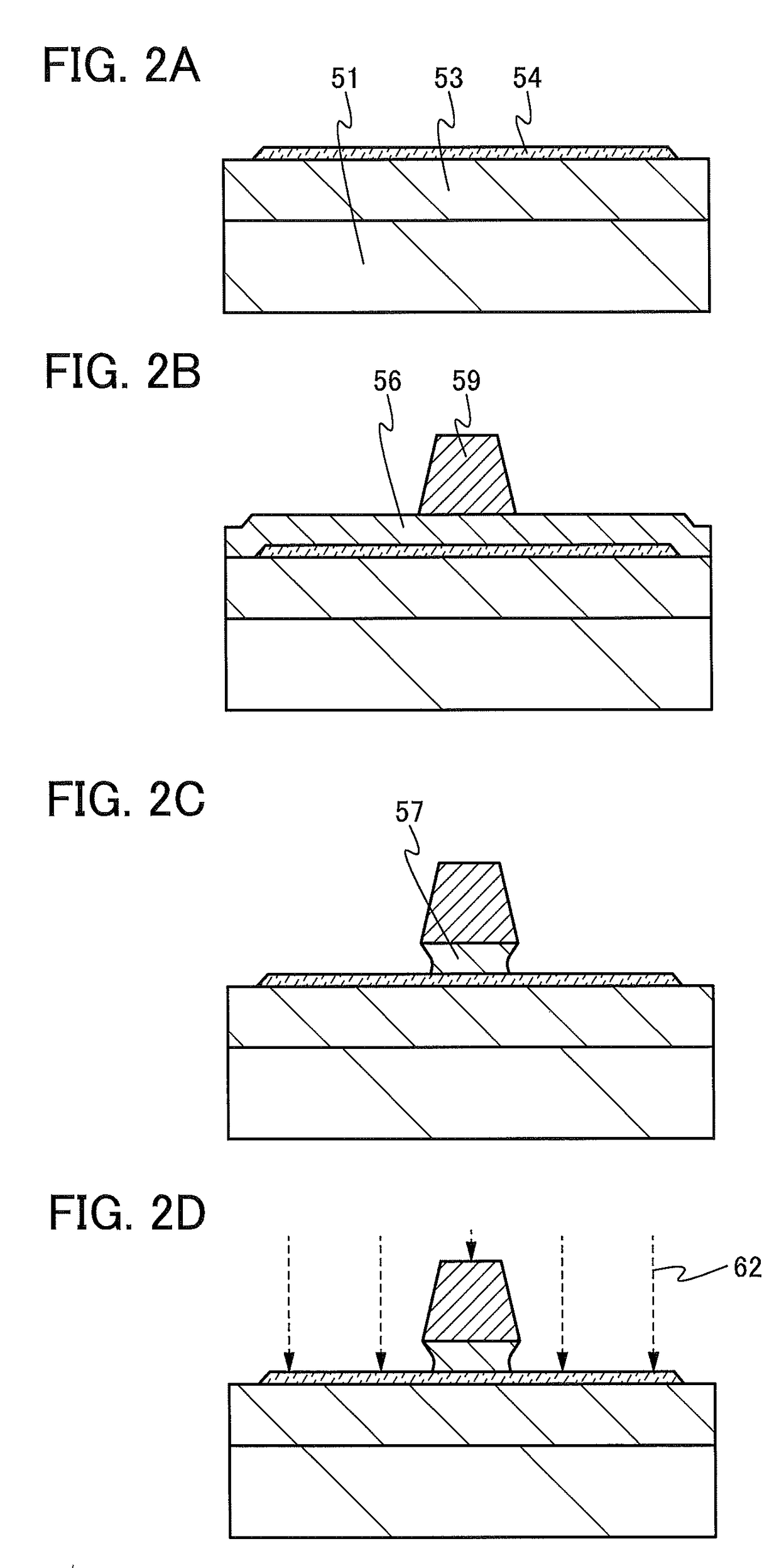
[0067]In this embodiment, one embodiment of a semiconductor device and a method for manufacturing the semiconductor device will be described with reference to FIGS. 1A to 1D, FIGS. 2A to 2D, and FIGS. 3A to 3C.

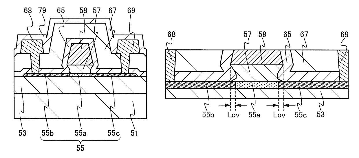
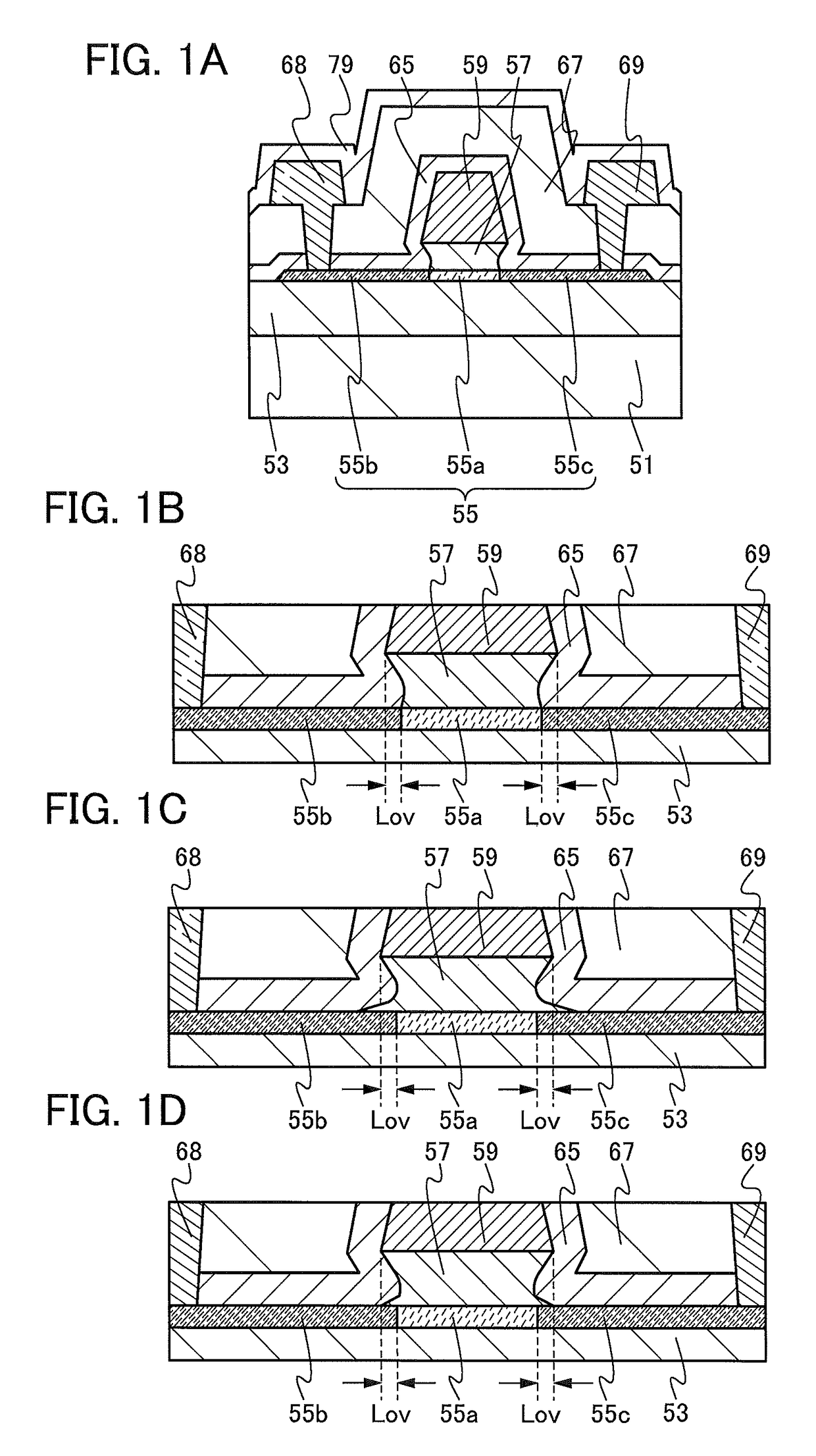
[0068]FIGS. 1A to 1D are each a cross-sectional view of a top-gate self-aligned transistor that is an example of a transistor in a semiconductor device.

[0069]The transistor illustrated in FIG. 1A includes an oxide semiconductor film 55, a gate insulating film 57 in contact with the oxide semiconductor film 55, and a gate electrode 59 in contact with the gate insulating film 57 and overlapping with the oxide semiconductor film 55.

[0070]The oxide semiconductor film 55 in the transistor is formed over an insulating film 53 that is formed over a substrate 51. In addition, an insulating film 65 containing hydrogen that is in contact with second regions 55b and 55c in the oxide semiconductor film 55 is provided.

[0071]Furthermore, an insulating film 67 in contact with t...

embodiment 2

(Embodiment 2)

[0178]In this embodiment, embodiments of a semiconductor device and a method for manufacturing the semiconductor device will be described with reference to FIGS. 4A to 4D, FIGS. 5A to 5D, and FIGS. 6A to 6C.

[0179]FIGS. 4A to 4D are cross-sectional views of top-gate self-aligned transistors that are examples of a transistor in a semiconductor device. Transistors described in this embodiment are different from those described in Embodiment 1 in that the gate insulating film has a stacked-layer structure.

[0180]The transistor illustrated in FIG. 4A includes an oxide semiconductor film 55, a gate insulating film 57 in contact with the oxide semiconductor film 55, and a gate electrode 59 in contact with the gate insulating film 57 and overlapping with the oxide semiconductor film 55. In the gate insulating film 57, a first insulating film 57a and a second insulating film 57b are stacked in this order from the oxide semiconductor film 55 side. That is, the first insulating fi...

embodiment 3

(Embodiment 3)

[0223]In this embodiment, a reduction in resistivity of the second regions 55b and 55c in the oxide semiconductor film 55 that occurs when the second regions 55b and 55c in the oxide semiconductor film 55 contain oxygen vacancies and hydrogen will be described. Specifically, VOH formed in the second regions 55b and 55c in the oxide semiconductor film 55 will be described. Note that in this embodiment, a state in which a hydrogen atom H exists in an oxygen vacancy VO is expressed as VOH.

OH>

[0224]In the case where an oxide semiconductor film (hereinafter referred to as IGZO) is a crystal, H preferentially diffuses along the a-b plane at a room temperature. In heat treatment at 450° C., H diffuses along the a-b plane and in the c-axis direction. Here, description is made on whether H easily enters an oxygen vacancy VO if the oxygen vacancy VO exists in IGZO.

[0225]An InGaZnO4 crystal model shown in FIG. 8 was used for calculation. The activation barrier (Ea) along the reac...


PUM


Abstract

A self-aligned transistor including an oxide semiconductor film, which has excellent and stable electrical characteristics, is provided. A semiconductor device is provided with a transistor that includes an oxide semiconductor film, a gate electrode overlapping with part of the oxide semiconductor film, and a gate insulating film between the oxide semiconductor film and the gate electrode. The oxide semiconductor film includes a first region and second regions between which the first region is positioned. The second regions include an impurity element. A side of the gate insulating film has a depressed region. Part of the gate electrode overlaps with parts of the second regions in the oxide semiconductor film.

Description

BACKGROUND OF THE INVENTION[0001]1. Field of the Invention[0002]The present invention relates to an object, a method, or a manufacturing method. In addition, the present invention relates to a process, a machine, manufacture, or a composition of matter. In particular, one embodiment of the present invention relates to a semiconductor device, a display device, a light-emitting device, a power storage device, a memory device, a driving method thereof, or a manufacturing method thereof. Specifically, one embodiment of the present invention relates to a semiconductor device including a field-effect transistor.[0003]In this specification and the like, a semiconductor device generally means a device that can function by utilizing semiconductor characteristics. A semiconductor element such as a transistor, a semiconductor circuit, an arithmetic device, and a memory device are each an embodiment of a semiconductor device. An imaging device, a display device, a liquid crystal display device,...

Claims


Application Information

Patent Timeline
Patent Type & Authority Patents(United States)
IPC IPC(8): H01L29/10H01L27/12H01L29/24H01L29/786H01L29/423H01L27/32
CPCH01L29/7869H01L27/1225H01L29/24H01L29/42384H01L29/78618H01L29/78696H01L27/3262H10K59/1213H01L29/42364H01L29/4908H01L29/66969
Inventor YAMAZAKI, SHUNPEISUZAWA, HIDEOMIJINTYOU, MASAMI
Owner SEMICON ENERGY LAB CO LTD
Why Eureka
Try Eureka