Heat dissipation approach in chip on board assembly by using stacked copper microvias

a technology of stacked copper microvias and chip on board, which is applied in the direction of semiconductor lasers, printed circuit non-printed electric components association, instruments, etc., can solve the problem of increasing the power consumption of optical transceivers within the interconnected nodes

Active Publication Date: 2017-05-02
GOOGLE LLC
View PDF12 Cites 23 Cited by
  • Summary
  • Abstract
  • Description
  • Claims
  • Application Information

AI Technical Summary

Problems solved by technology

The increased amount of data transmission increases the power consumption of the optical transceivers within the interconnected nodes.

Method used


Image

  • Heat dissipation approach in chip on board assembly by using stacked copper microvias
  • Heat dissipation approach in chip on board assembly by using stacked copper microvias
  • Heat dissipation approach in chip on board assembly by using stacked copper microvias

Examples


Embodiment Construction

[0013]The various concepts introduced above and discussed in greater detail below may be implemented in any of numerous ways, as the described concepts are not limited to any particular manner of implementation. Examples of specific implementations and applications are provided primarily for illustrative purposes.

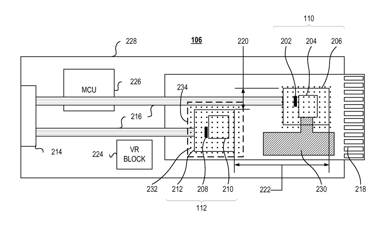
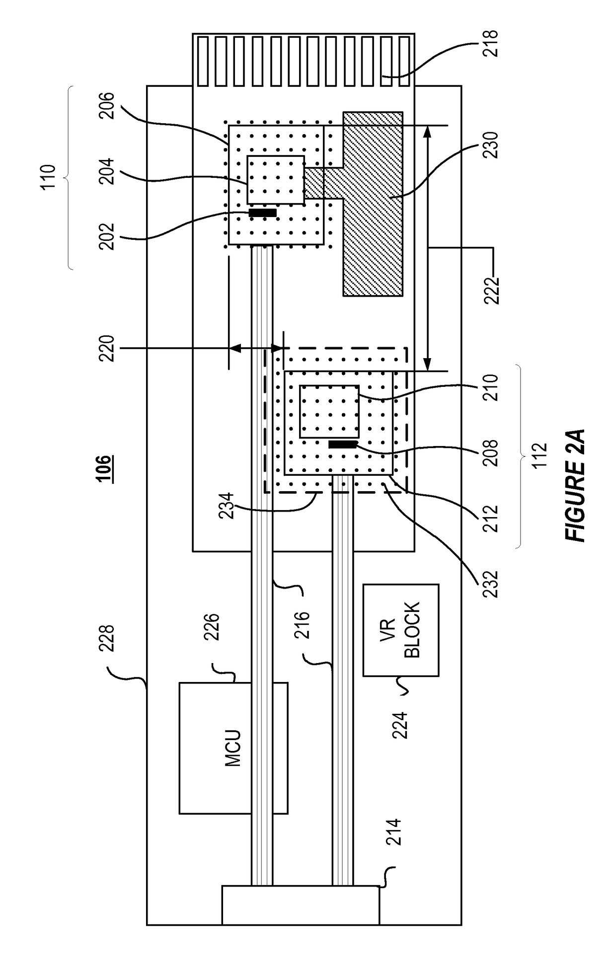
[0014]As an overview, as the data transfer rate of optical transceivers increases, the power required to operate the optical transceivers increases. The increase in power consumption can result in higher operating temperatures. Laser output can be impacted by temperature, and thus excessive operating temperatures can degrade transceiver performance. The present disclosure increases optical transceiver performance by reducing operating temperatures by placing a plurality of thermal microvias under the components of the optical transceiver. A standard printed circuit board is a poor conductor of thermal energy. Accordingly, the heat generated by the components of the optical ...


PUM

PropertyMeasurementUnit
diameteraaaaaaaaaa
diameteraaaaaaaaaa
diameteraaaaaaaaaa

Abstract

The present disclosure discusses an improved optical transceiver. The optical transceiver of the present disclosure includes an optical transmitter and an optical receiver coupled to an area of a printed circuit board that includes a plurality of thermal microvias. The thermal microvias are coupled to a heat sink or other heat dissipater and provide a path from the components of the optical transceiver to the heat dissipater for heat to travel.

Description

CROSS-REFERENCE TO RELATED APPLICATIONS[0001]This application claims priority to U.S. Provisional Patent Application No. 62 / 062,476 filed on Oct. 10, 2014 and titled “Novel Heat Dissipation Approach In Chip On Board Assembly By Using Stacked Copper Microvias,” which is herein incorporated by reference in its entirety.BACKGROUND OF THE DISCLOSURE[0002]Datacenter networks include a plurality of interconnected nodes. In some datacenters, the nodes are interconnected by optical links. The amount of data passed between the interconnected nodes is increasing. The increased amount of data transmission increases the power consumption of the optical transceivers within the interconnected nodes.SUMMARY OF THE DISCLOSURE[0003]According to one aspect of the disclosure, an optical transceiver includes an optical transmitter with a first chip-on-board package coupled to a printed circuit board (PCB) and an optical receiver including a second chip-on-board package coupled to the PCB. The PCB inclu...

Claims


Application Information

Patent Timeline
Patent Type & Authority Patents(United States)
IPC IPC(8): H04B10/40B23K26/38H05K3/00H05K3/30H05K1/02
CPCH04B10/40H05K1/0206B23K26/381H05K3/0047H05K3/0094H05K3/30B23K26/382G02B6/32G02B6/4204G02B6/4246G02B6/4269G02B6/428G02B6/00H05K1/0274H05K2201/10121H05K2201/10416H01S5/0261H04B10/801H05K1/18H05K3/061H05K3/32H05K3/4038
Inventor SHEN, ZUOWEIFUKUCHI, KYLEBEAUCHEMIN, MELANIEURATA, RYOHEI
Owner GOOGLE LLC
Why Eureka
Try Eureka