Electrostatic discharge protection semiconductor device

a technology of protection semiconductor and electrostatic discharge, which is applied in the direction of semiconductor devices, diodes, electrical equipment, etc., can solve the problems of increasing the vulnerability of esd to the impact of external environment, and the constant threat of esd to modern electronics, so as to reduce the threshold voltage improve device robustness and improve product flexibility and functionality of esd protection semiconductor devices

Active Publication Date: 2017-05-16
UNITED MICROELECTRONICS CORP
View PDF6 Cites 8 Cited by
  • Summary
  • Abstract
  • Description
  • Claims
  • Application Information

AI Technical Summary

Benefits of technology

[0009]According to the ESD protection semiconductor device provided by the present invention, the first doped region including the first conductivity type or, alternatively, the second conductivity type is formed in the source region or in the drain region. And the first doped region is electrically connected to the ground potential. Accordingly, a diode or a bipolar junction transistor (hereinafter abbreviated as BJT) is formed in the substrate, therefore the threshold voltage of the ESD protection semiconductor device is reduced while the turn-on speed and the device robustness of the ESD protection semiconductor device are improved. Furthermore, the ESD protection semiconductor device provided by the present invention includes the gate set, and the gate set can include single gate, multi gate, or multi gate group. Therefore, the ESD protection semiconductor device provided by the present invention is able to be integrated into single-gate metal-oxide-semiconductor (hereinafter abbreviated as MOS) transistor device, cascode transistor device, multi-gate MOS transistor, and fin field effect transistor (hereinafter abbreviated as FinFET). Additionally, by forming well regions of different conductivity types in the substrate, the ESD protection semiconductor device provided by the present invention is able to be integrated with lateral-diffusion metal-oxide-semiconductor (hereinafter abbreviated as LDMOS) transistor approach. In other words, the ESD protection semiconductor device provided by the present invention is able to be integrated with various transistor approaches, thus product flexibility and functionality of the ESD protection semiconductor device are both improved.

Problems solved by technology

As products based on ICs become more delicate, they also become more vulnerable to the impacts from external environment.
And thus, it is assumed that ESD is a constant threat to the modern electronics.

Method used


Image

  • Electrostatic discharge protection semiconductor device
  • Electrostatic discharge protection semiconductor device
  • Electrostatic discharge protection semiconductor device

Examples


Embodiment Construction

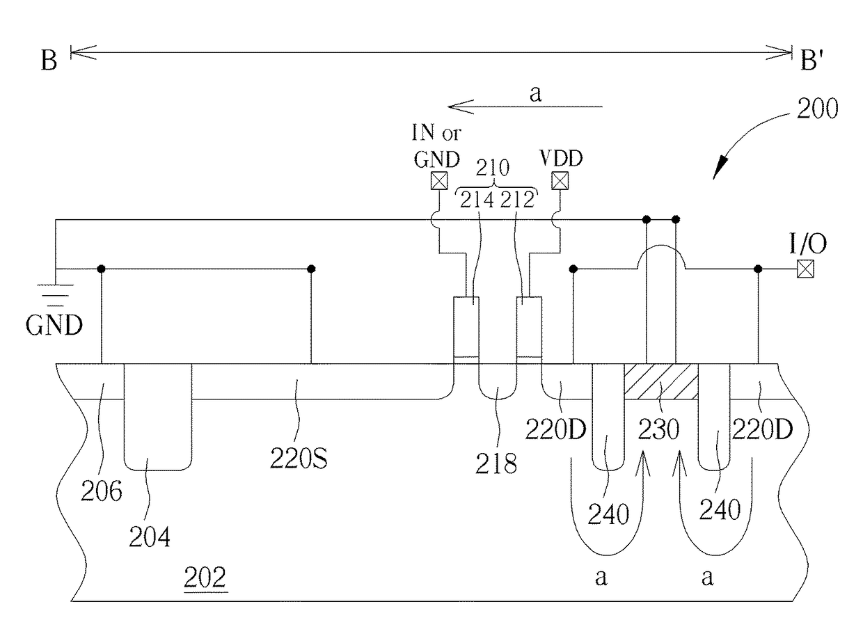
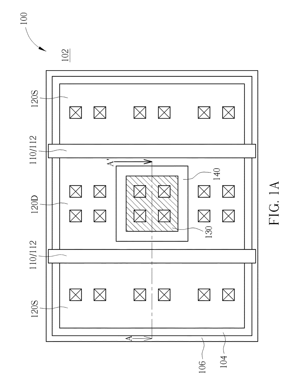
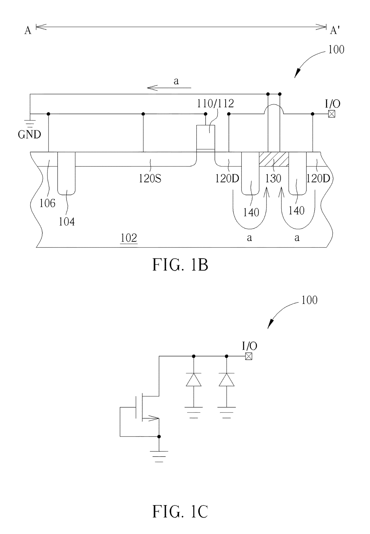
[0036]Please refer to FIGS. 1A-1C, wherein FIG. 1A is a schematic drawing illustrating a layout structure of an ESD protection semiconductor device provided by a first preferred embodiment of the present invention, FIG. 1B is a schematic drawing illustrating the ESD protection semiconductor device provided by the first preferred embodiment and also is a cross-sectional view taken along a Line A-A′ of FIG. 1A, and FIG. 1C is a circuit diagram of the ESD protection semiconductor device provided by the first preferred embodiment. As shown in FIG. 1A and FIG. 1B, the ESD protection semiconductor device 100 provided by the preferred embodiment includes a substrate, and the substrate includes a well region 102. A gate set 110 is positioned on the substrate and the well region 102. In the preferred embodiment, the gate set 110 includes a single gate structure 112. It is well-known to those skilled in the art that the single gate structure 112 includes a gate conductive layer and a gate die...


PUM


Abstract

An ESD protection semiconductor device includes a substrate, a gate set formed on the substrate, a source region and a drain region formed in the substrate respectively at two sides of the gate set, and at least a first doped region formed in the drain region. The source region and the drain region include a first conductivity type, and the first doped region includes a second conductivity type. The first conductivity type and the second conductivity type are complementary to each other. The first doped region is electrically connected to a ground potential.

Description

BACKGROUND OF THE INVENTION[0001]1. Field of the Invention[0002]The invention relates to an electrostatic discharge (hereinafter abbreviated as ESD) protection semiconductor device.[0003]2. Description of the Prior Art[0004]With the advancement of technology, the development of semiconductor process is ongoing. A modern chip is therefore allowed to have a plurality of various electronic circuits configured within. For example, the integrated circuits (ICs) integrated in the chip(s) can be divided into core circuits and input / output (hereinafter abbreviated as I / O) circuits, and the core circuits and the I / O circuits are respectively driven by different power supply sources with different voltages. And for receiving the externally provided power, pads for core circuits and I / O circuits are required.[0005]However, it is found that electrostatic charges are easily transferred to the inner circuits in the chip by those pads during processes such as manufacturing, testing, packaging, and...

Claims


Application Information

Patent Timeline
Patent Type & Authority Patents(United States)
IPC IPC(8): H01L27/02H01L29/06H01L29/78
CPCH01L27/0255H01L29/0653H01L29/7819H01L29/7851H01L27/027H01L29/7835H01L29/0696H01L29/1087H01L29/7831H01L29/0847H01L29/1045H01L27/0207H01L29/0649H01L29/785
Inventor HUANG, CHUNG-YUSU, KUAN-CHENGTANG, TIEN-HAOCHEN, PING-JUILAI, PO-YA
Owner UNITED MICROELECTRONICS CORP
Why Eureka
Try Eureka