Varactor device with backside contact

a capacitor and backside contact technology, applied in semiconductor devices, diodes, electrical apparatuses, etc., can solve the problems of reducing the performance of the transceiver, reducing the contact resistance, reducing the device performance, etc., to improve the signal loss and operation of the device, reduce the impedance, and the effect of shortening the length

Active Publication Date: 2017-05-23
QUALCOMM INC
View PDF13 Cites 3 Cited by
  • Summary
  • Abstract
  • Description
  • Claims
  • Application Information

AI Technical Summary

Benefits of technology

[0004]A varactor device may include a first contact positioned on a front side of a substrate and a second contact (e.g., a backside contact) positioned on a backside of the substrate. Use of the backside contact may reduce an impedance associated with the varactor device, which may improve device signal loss and operation. To illustrate, a radio frequency (RF) signal may be conducted via a signal path between the first contact and the second contact, and the signal path may have a shorter length (and less impedance) as compared to an RF signal path of a varactor that uses two front-side contacts through semiconductor material. Thus, use of the backside contact may reduce attenuation of the RF signal. In a particular embodiment, the varactor device is integrated within a transceiver.
[0005]The varactor device may further include a third contact and a fourth contact. The third contact and the fourth contact may be responsive to a bias voltage to change a size of one or more depletion regions of the varactor device. By changing the size of a depletion region, a width of the signal path of the varactor device may be changed, enabling control of the capacitance of the varactor. In this example, a width of a “plate” of a capacitive region of the varactor device may be adjusted, which may enable more precise capacitance control as compared to a device that adjusts only a distance between “plates” of a capacitive region.
[0006]In addition, the RF signal and the bias voltage may be separately applied to the varactor device using the first contact, the third contact, and the fourth contact. For example, instead of applying both an RF signal and a bias voltage to a single pair of contacts, the RF signal may be applied to the first contact, and the bias voltage may be applied to the third contact and to the fourth contact. Separately applying an RF signal and a bias voltage may improve response linearity as compared to a two-port varactor device that applies both an RF signal and a bias voltage to a single pair contacts. For example, use of the third contact and the fourth contact may enable more precise biasing control by avoiding “mixing” of an RF signal and a bias voltage (which can cause nonlinearity of device operation).
[0011]One particular advantage provided by at least one of the disclosed embodiments is reduced RF signal attenuation at a varactor device. For example, use of a backside contact may reduce a length of a signal path between contacts of the varactor device, thus reducing impedance and signal loss. Another particular advantage provided by at least one of the disclosed embodiments is reduced contact resistance. For example, a high-conductivity material of the backside contact may reduce contact resistance. Another particular advantage provided by at least one of the disclosed embodiments is enhanced linearity of response to a bias voltage. For example, by changing a size of a depletion region of the varactor device, capacitance of the varactor device may be controlled more accurately (and more linearly) as compared to other varactors. Other aspects, advantages, and features of the present disclosure will be described or become apparent after review of the entire application, including the following sections: Brief Description of the Drawings, Detailed Description, and the Claims.

Problems solved by technology

In some implementations, operation of a varactor may deviate substantially from “ideal” varactor behavior, which may reduce performance of the transceiver.
In this case, capacitance of the varactor may be imprecisely controlled, which may reduce device performance (e.g., due to increased current dissipation caused by poor tuning of the varactor, or increased non-linearity to distort signal).
For example, a high-conductivity material of the backside contact may reduce contact resistance.

Method used


Image

  • Varactor device with backside contact
  • Varactor device with backside contact
  • Varactor device with backside contact

Examples


Embodiment Construction

[0018]Particular examples are described below with reference to the drawings. Similar or common features are designated by common reference numbers throughout the description and the drawings.

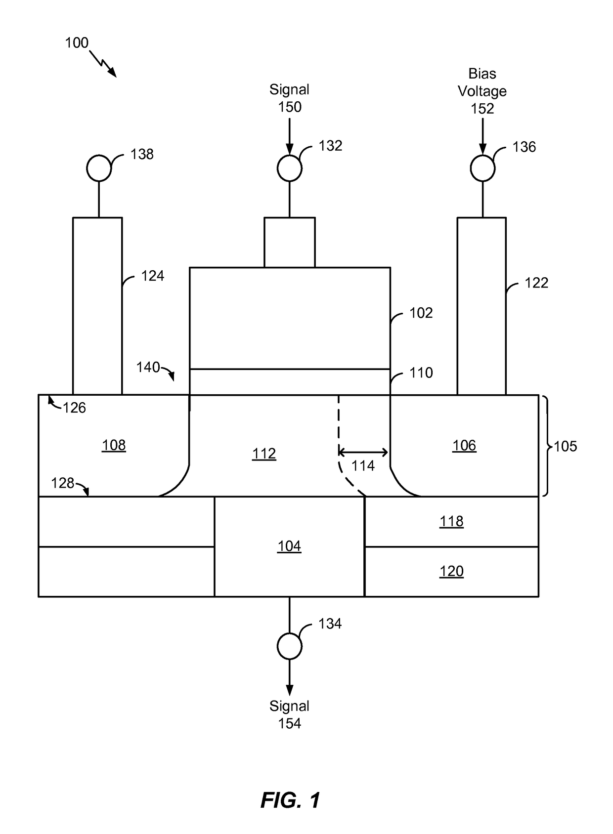
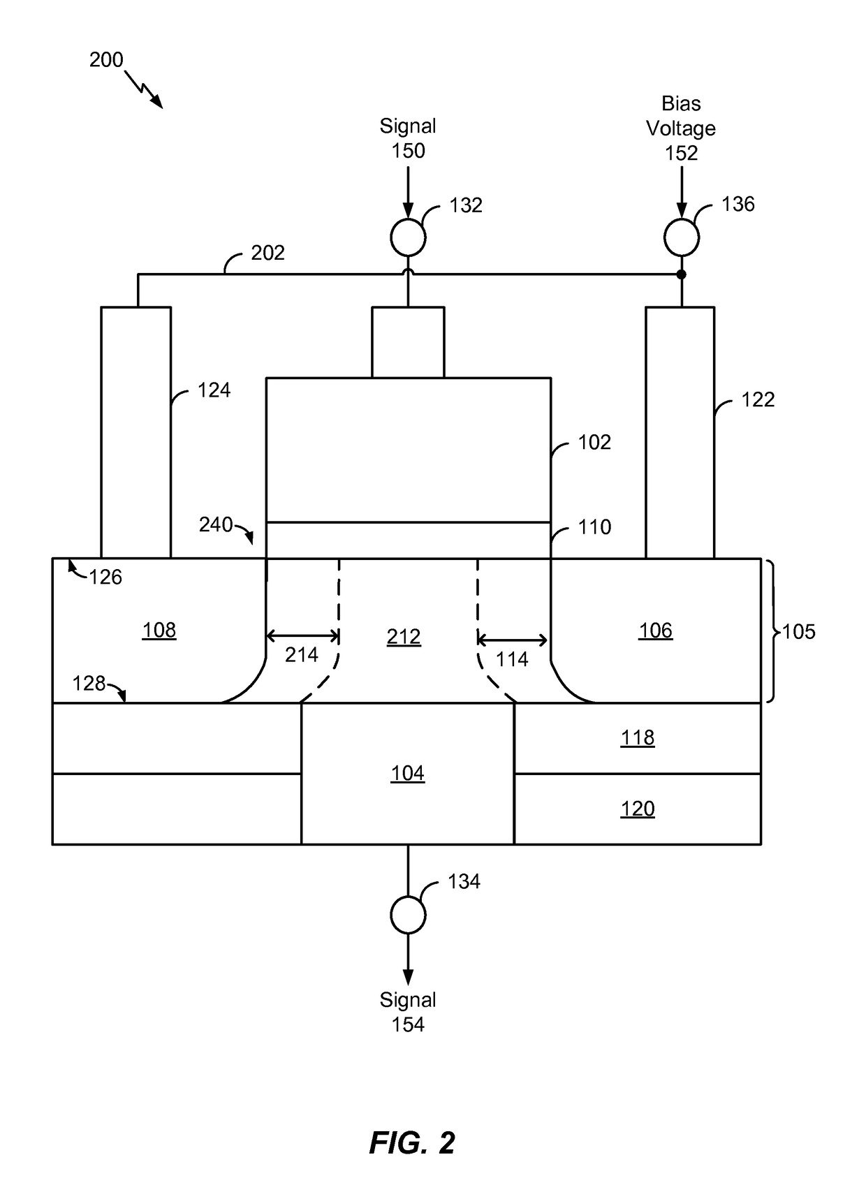
[0019]Referring to FIG. 1, a particular illustrative embodiment of a variable capacitor (varactor) device is depicted and generally designated 100. The varactor device 100 may be integrated within an electronic device, such as within a transceiver, as an illustrative example. To further illustrate, the transceiver (e.g., a receiver front-end of the transceiver) may include one or more varactor devices corresponding to the varactor device 100. The transceiver may utilize the one or more varactor devices to tune to receive and transmit one or more signals that are conveyed using a particular frequency or frequency band. In this example, the one or more varactors may have a frequency response that filters received signals, such as by suppressing or reducing certain low-frequency signal components....


PUM


Abstract

An apparatus includes a varactor having a first contact that is located on a first side of a substrate. The varactor includes a second contact that is located on a second side of the substrate, and the second side is opposite the first side. The apparatus further includes a signal path between the first contact and the second contact.

Description

I. FIELD[0001]The present disclosure is generally related to variable capacitor (varactor) devices.II. DESCRIPTION OF RELATED ART[0002]Advances in technology have resulted in smaller and more powerful computing devices. For example, there currently exist a variety of portable personal computing devices, including wireless telephones such as mobile and smart phones, tablets and laptop computers that are small, lightweight, and easily carried by users. These devices can communicate voice and data packets over wireless networks. Further, many such devices incorporate additional functionality such as a digital still camera, a digital video camera, a digital recorder, and an audio file player. Also, such devices can process executable instructions, including software applications, such as a web browser application, that can be used to access the Internet. As such, these devices can include significant computing capabilities.[0003]Wireless telephones and other electronic devices may inclu...

Claims


Application Information

Patent Timeline
Patent Type & Authority Patents(United States)
IPC IPC(8): H01L29/93H01L29/94H01L27/06
CPCH01L29/93H01L29/94H01L27/0629
Inventor KIM, DAEIK DANIELKIM, JONGHAEZUO, CHENGJIEPARK, SANG-JUNEYUN, CHANGHAN HOBIEVELEZ, MARIO FRANCISCOBERDY, DAVID FRANCISNOWAK, MATTHEW MICHAELMIKULKA, ROBERT PAUL
Owner QUALCOMM INC
Why Eureka
Try Eureka