Check patentability & draft patents in minutes with Patsnap Eureka AI!

Systems and methods for testing circuitry programmability

a circuit and programmability technology, applied in the field of circuitry testing functionality, can solve the problems of increasing the problem of scan chain testing technique, not being ideal for all circuit configurations, and not being able to implement such programmability within various circuitry, so as to reduce test time/and, increase coverage, and reduce test cost significantly

Inactive Publication Date: 2017-05-30
CSR TECH INC
View PDF8 Cites 1 Cited by
  • Summary
  • Abstract
  • Description
  • Claims
  • Application Information

AI Technical Summary

Benefits of technology

This method enables rapid, cost-effective testing of circuit programmability, reducing test time and costs, and providing more comprehensive coverage than traditional methods, especially for digital programmability embedded in analog circuitry, by detecting small voltage changes with moderate / low resolution ADCs and on-chip implementation.

Problems solved by technology

Although such programmability may be desirable in providing flexibility with respect to the functionality provided, implementing such programmability within various circuitry is not without difficulty.
As more and more programmability is introduced to the various circuits, the problem of testing the circuits grows exponentially.
Although such a scan chain provides a relatively fast testing technique, whereby simple test patterns may be utilized to detect stuck faults with respect to digital circuitry, such a scan chain testing technique is not ideal for all circuit configurations.
For example, circuitry in which a full scan design cannot be implemented (e.g., circuitry having sequential circuits, such as memory elements that are not part of the scan chain) require sequential pattern generation for testing resulting in more complex and time consuming testing.
Moreover, the scan chain testing technique can only be implemented through a purely digital circuit.
When the circuitry under test comprises a digital block which is deeply embedded inside an analog block, the use of a scan chain becomes problematic if not impossible.
However, the introduction of such a boundary testing configuration is only possible for non-sensitive and non-critical nodes where adding an additional flip-flop and the associated loading is not an issue with respect to the normal, non-test mode operation of the circuit under test.
Moreover, a boundary test implementation is not possible with respect to all circuit configurations.
However, such a test point implementation is very likely to introduce ground noise.
The introduction of such ground noise would require multiple samples to be captured for averaging, thereby requiring longer testing times. Moreover, since a larger out of circuit load must be charged, each sample capture would be slower.
However, such functional tests are also typically not ideal.
In particular, it is generally expensive and very time consuming to perform a full functional test of circuitry, particularly if a functional mode must be implemented in order to test just for logical errors in the programmability.
Moreover, some minor programmability (e.g., bias current control) may not have any significant change in output parameter and thus the programmability may not be observable at all using a functional test.

Method used


Image

  • Systems and methods for testing circuitry programmability
  • Systems and methods for testing circuitry programmability
  • Systems and methods for testing circuitry programmability

Examples


Embodiment Construction

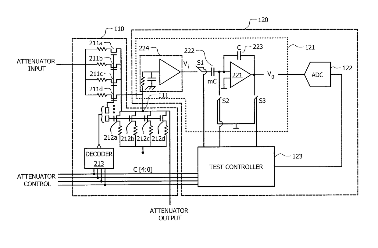
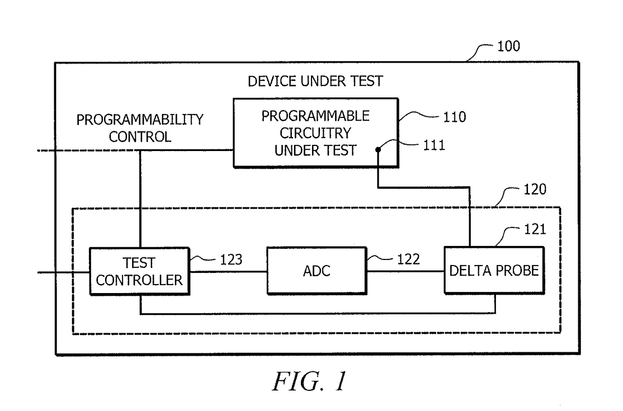
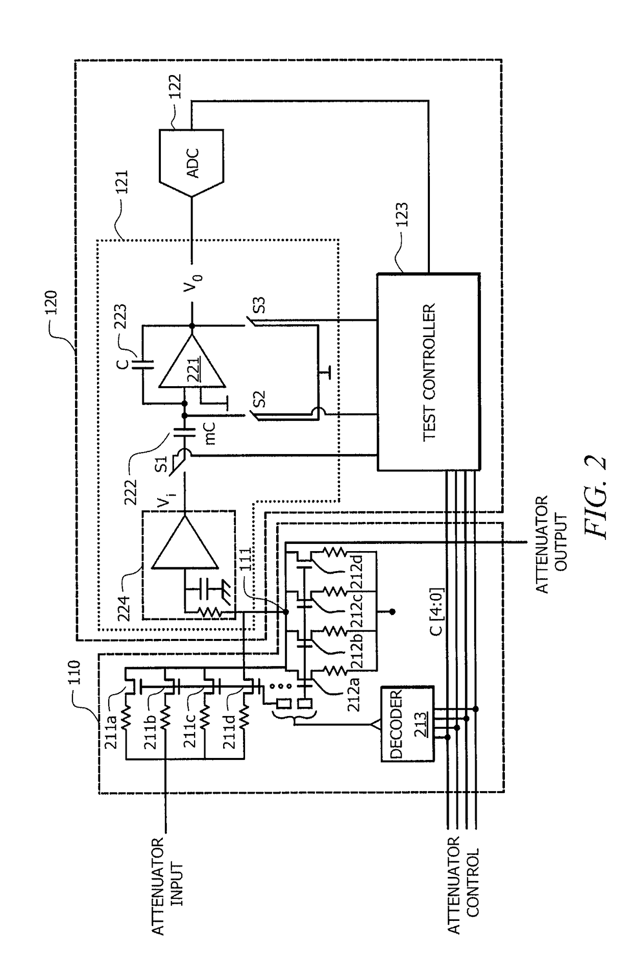
[0022]FIG. 1 shows a device as may be provided testing using testing circuitry adapted according to embodiments of the invention. In particular, FIG. 1 shows device under test (DUT) 100 which may comprise one or more programmable circuit (shown here as programmable circuitry under test (PCUT) 110) for which testing is provided according to the concepts herein by delta test circuitry 120. DUT 100 may, for example, comprise an integrated circuit used in various consumer and professional devices, such as cellular telephones, smart phones, PDAs, tablet devices, computer systems, video displays, televisions, set top boxes, digital video recorders, network devices, etc., having programmability to facilitate configuring of features and / or selection of particular features available using the circuitry. Such programmability may utilize digitally programmable analog blocks (e.g., analog circuits that perform functions such as automatic gain control, band selection, filter pole re-adjustment, ...


PUM


Abstract

Systems and methods in which circuitry programmability is tested through observing a change in voltage on a circuit node that is affected by the programmability under test. For example, one or more particular circuit node may be identified at which some measurable change in voltage occurs upon a change in state of a programmable circuit under test (PCUT). Thus, by detecting a change in voltage at such a circuit node in association with a programmable state change, embodiments may determine that respective circuit programmability is functional. Test circuitry of embodiments provides for circuitry programmability testing, through observing a change in voltage on a circuit node that is affected by the programmability under test, suitable for testing digital programmability which is deeply embedded in analog circuitry.

Description

TECHNICAL FIELD[0001]The present invention relates generally to circuitry testing functionality and, more particularly, to testing circuitry programmability.BACKGROUND OF THE INVENTION[0002]The state of electronics has advanced to a point in which various, often complex features are implemented by a particular circuit configuration. For example, the integrated circuits forming various consumer and professional devices, such as cellular telephones, smart phones, personal digital assistants (PDAs), tablet devices, computer systems, video displays, televisions, set top boxes, digital video recorders, network devices, etc., are often adapted to not only implement robust features but may implement a plurality of different features.[0003]Various programmability may be provided in the circuit implementation to facilitate configuring of features and / or selection of particular features available using the circuitry. Such programmability may be provided in an integrated circuit configuration,...

Claims


Application Information

Patent Timeline
Patent Type & Authority Patents(United States)
IPC IPC(8): G01F19/00G01R31/3185G01R19/00
CPCG01R31/318516G01R19/0084G01R31/2836G01R31/3167
Inventor SHRIVASTAVA, AYASKANT
Owner CSR TECH INC
Features
  • R&D
  • Intellectual Property
  • Life Sciences
  • Materials
  • Tech Scout
  • Unparalleled Data Quality
  • Higher Quality Content
  • 60% Fewer Hallucinations
Learn More