Fast and low-power sense amplifier and writing circuit for high-speed MRAM

a writing circuit and high-speed mram technology, applied in information storage, static storage, digital storage, etc., can solve the problems of small available sensing margin, difficult to determine the switching direction, and many new challenges, and achieve fast read and write operations, reduce write power consumption, and minimize the bit error rate

Active Publication Date: 2017-06-06
RGT UNIV OF CALIFORNIA
View PDF1 Cites 6 Cited by
  • Summary
  • Abstract
  • Description
  • Claims
  • Application Information

AI Technical Summary

Benefits of technology

[0013]A high-speed and low-power pre-read and write sense amplifier (PWSA) is described for magnetoresistive random access memory (MRAM). The sense amplifier incorporates a writing circuit for MRAM bits switched via timing of precessional dynamics (approximately GHz speed) in a magnetic tunnel junction (MTJ). By combining read and write functions in a single power-efficient circuit, the PWSA allows for fast read and write operations while minimizing the bit error rate (BER) after data programming. In the embodiment described, the PWSA circuit is designed based on a 65 nm CMOS technology, although it will be appreciated that the disclosed circuit approach is applicable to other circuit technologies and feature dimensions. The approach has been tested with magnetic dynamics captured by a Verilog-A compact model based on macrospin behavior for MTJs. Using the pre-read and comparison steps in the data program operation, the disclosed approach provides reduction in write power consumption by up to 50% under random data input conditions. Furthermore, by using the voltage controlled magnetic anisotropy (VCMA) effect for precessional switching, more than 10× reduction of write power and transistor size both in the memory cell and the write circuit is achieved, compared to using the spin transfer torque (STT) effect. The circuit achieves 2 ns read time, 1.8 ns write time, and 8 ns total data program operation time (consisting of two Read steps, one Write step and a Pass / Fail check step) by using this PWSA concept and a 2× larger sensing margin through the current feedback circuit.

Problems solved by technology

However, it also presents a number of new challenges.
The first one is difficulty in determining the switching direction.
However, the available sensing margin is small due to the low tunneling magnetoresistance (TMR) of the 1T-1 MTJ memory architecture: i.e., the series bit line (BL) resistance decreases the resistance ratio of MTJs seen by the sensing circuitry.
Furthermore, since a bias across the MTJ reduces its resistance, especially the resistance in the anti-parallel state, the TMR is diminished compared to the case of zero biased.
This reduction further lowers the sensing margin, causing an increased possibility of an erroneous read.

Method used


Image

  • Fast and low-power sense amplifier and writing circuit for high-speed MRAM
  • Fast and low-power sense amplifier and writing circuit for high-speed MRAM
  • Fast and low-power sense amplifier and writing circuit for high-speed MRAM

Examples


Embodiment Construction

1. Introduction

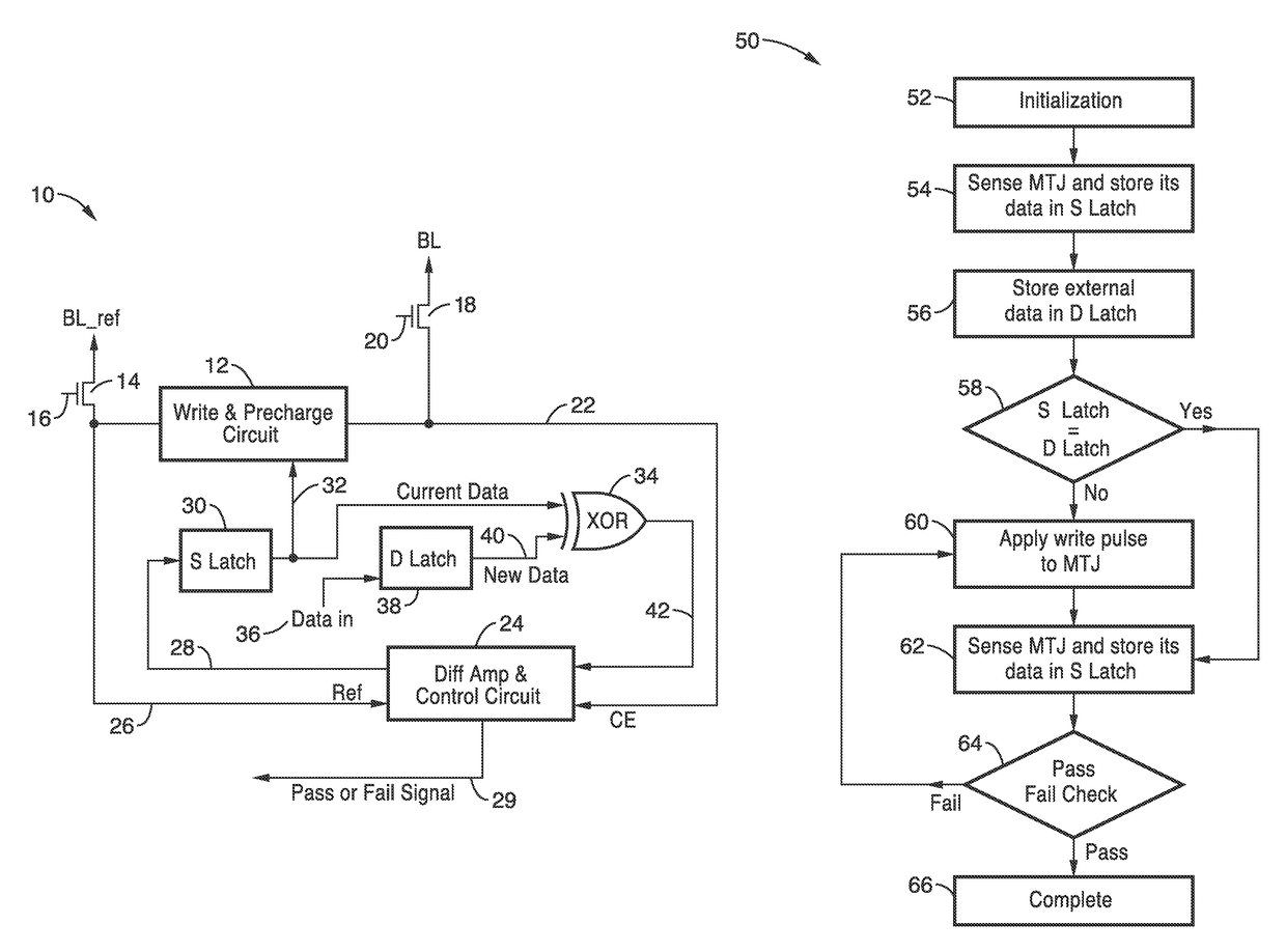
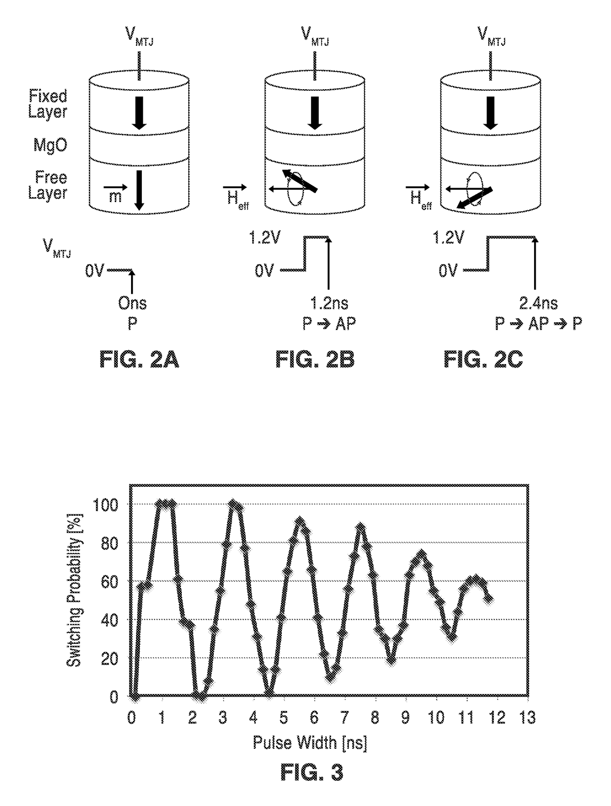
[0025]The present technology provides a number of benefits for MTJ memory cells including, but not limited to, the following abilities: (i) to enable reliable precessional programming for high-speed operation, by reducing the BER, while allowing for a large write error rate (WER) (up to 1%) of the precessional switching process; (ii) to reduce write power by utilizing a pre-read process for eliminating redundant writes; and (iii) to increase the sensing margin for reliable read operation by using a current feedback circuit.

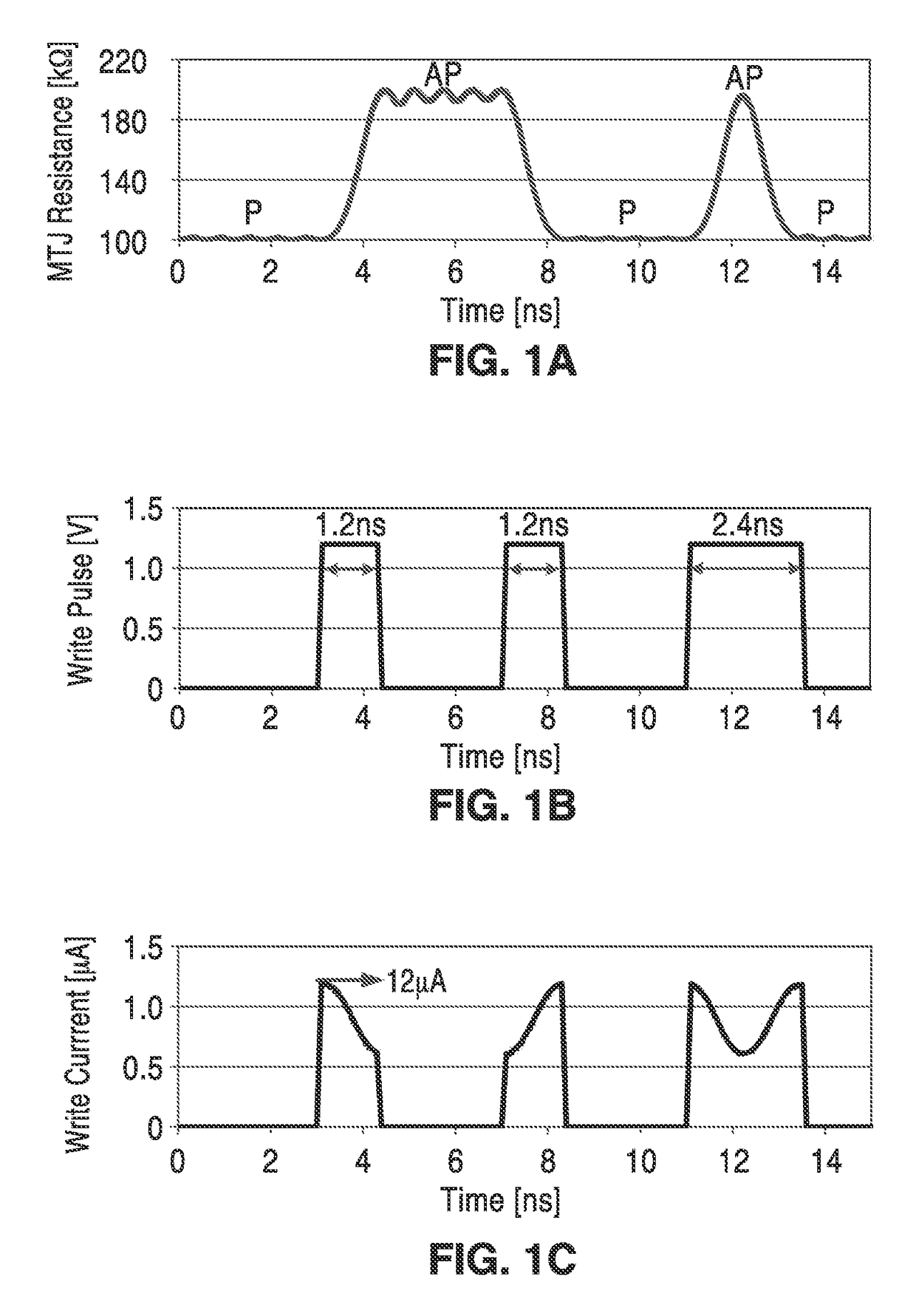
[0026]In the present disclosure, the bit error rate (BER) is defined as the number of bit errors divided by the total number of programmed bits after a full data program operation. Each full data program operation, in turn, may consist of multiple write operations into an individual bit. The acceptable bit error rate (ABER) is the maximum BER which can be corrected by error-correction code (ECC) techniques. The write error rate (WER), in turn, is de...


PUM


Abstract

A fast and low-power sense amplifier and writing circuit for high-speed Magnetic RAM (MRAM) which provides the long retention times and endurance of magnetic tunnel junction (MTJ) cells, while providing faster access speeds, verified writes, and an increased sensing margin. A high-speed and low-power pre-read and write sense amplifier (PWSA) provide VCMA effect precessional switching of MTJ cells which include pre-read and comparison steps which reduce power consumption. An embodiment of the PWSA circuit is described with write and pre-charge circuit, S and D latches, comparison circuit, and a differential amplifier and control circuit.

Description

CROSS-REFERENCE TO RELATED APPLICATIONS[0001]This application claims priority to, and the benefit of, U.S. provisional patent application Ser. No. 61 / 988,518 filed May 5, 2014, incorporated herein by reference in its entirety.STATEMENT REGARDING FEDERALLY SPONSORED RESEARCH OR DEVELOPMENT[0002]This invention was made with Government support under HR0011-10-C-0153, awarded by the U.S. Department of Defense, Defense Advanced Research Projects Agency. The Government has certain rights in the invention.INCORPORATION-BY-REFERENCE OF COMPUTER PROGRAM APPENDIX[0003]Not ApplicableNOTICE OF MATERIAL SUBJECT TO COPYRIGHT PROTECTION[0004]A portion of the material in this patent document is subject to copyright protection under the copyright laws of the United States and of other countries. The owner of the copyright rights has no objection to the facsimile reproduction by anyone of the patent document or the patent disclosure, as it appears in the United States Patent and Trademark Office publ...

Claims


Application Information

Patent Timeline
Patent Type & Authority Patents(United States)
IPC IPC(8): G11C11/00G11C11/16
CPCG11C11/1673G11C11/16G11C11/161G11C11/1675G11C7/065G11C11/1677G11C11/1693
Inventor WANG, KANG L.AMIRI, PEDRAM KHALILILEE, HOCHULALZATE, JUAN G.
Owner RGT UNIV OF CALIFORNIA
Why Eureka
Try Eureka