Light-emitting element, light-emitting device, electronic device, and lighting device including semi-transmissive and semi-reflective electrodes

a technology of light-emitting elements and electronic devices, which is applied in the direction of basic electric elements, semiconductor devices, electrical apparatus, etc., to achieve the effects of low power consumption, low viewing angle dependence of chromaticity and luminance, and high purity

Active Publication Date: 2017-06-27
SEMICON ENERGY LAB CO LTD
View PDF28 Cites 13 Cited by
  • Summary
  • Abstract
  • Description
  • Claims
  • Application Information

AI Technical Summary

Benefits of technology

[0011]Compared to the side-by-side patterning, high definition can be easily achieved by the white-color filter method because a plurality of light-emitting elements giving different emission colors (e.g., red, green, and blue) shares one light-emitting layer. Further, higher definition can be achieved by adoption of a top emission structure with which a high aperture ratio can be easily achieved compared to the case of a bottom emission structure. Thus, it can be said that a combination of the white-color filter method and a top emission structure (hereinafter referred to as a white-color filter top emission structure) is a suitable display method for display market where high definition is still demanded.
[0012]In the light-emitting device with such a white-color filter top emission structure, when a white-emissive light-emitting element is added to red-, green-, and blue-emissive light-emitting elements, power consumption can also be reduced. However, viewing angle dependence of chromaticity of the white-emissive light-emitting element is large compared with the red-, green-, and blue-emissive light-emitting elements.
[0015]The optical path lengths between the upper electrode and the lower electrode are independently adjusted in the red-, green-, and blue-emissive light-emitting elements so that emission of the corresponding color is amplified; therefore, both front luminance and color purity can be improved. However, in the white-emissive light-emitting element, it is difficult to obtain white light emission if a specific emission is amplified.

Problems solved by technology

However, a transparent conductive film typified by ITO has high resistance among conductive materials used as an electrode material; thus, the upper electrode is generally formed using a combination of the transparent conductive film and a metal thin film with low resistance.

Method used


Image

  • Light-emitting element, light-emitting device, electronic device, and lighting device including semi-transmissive and semi-reflective electrodes
  • Light-emitting element, light-emitting device, electronic device, and lighting device including semi-transmissive and semi-reflective electrodes
  • Light-emitting element, light-emitting device, electronic device, and lighting device including semi-transmissive and semi-reflective electrodes

Examples


embodiment 1

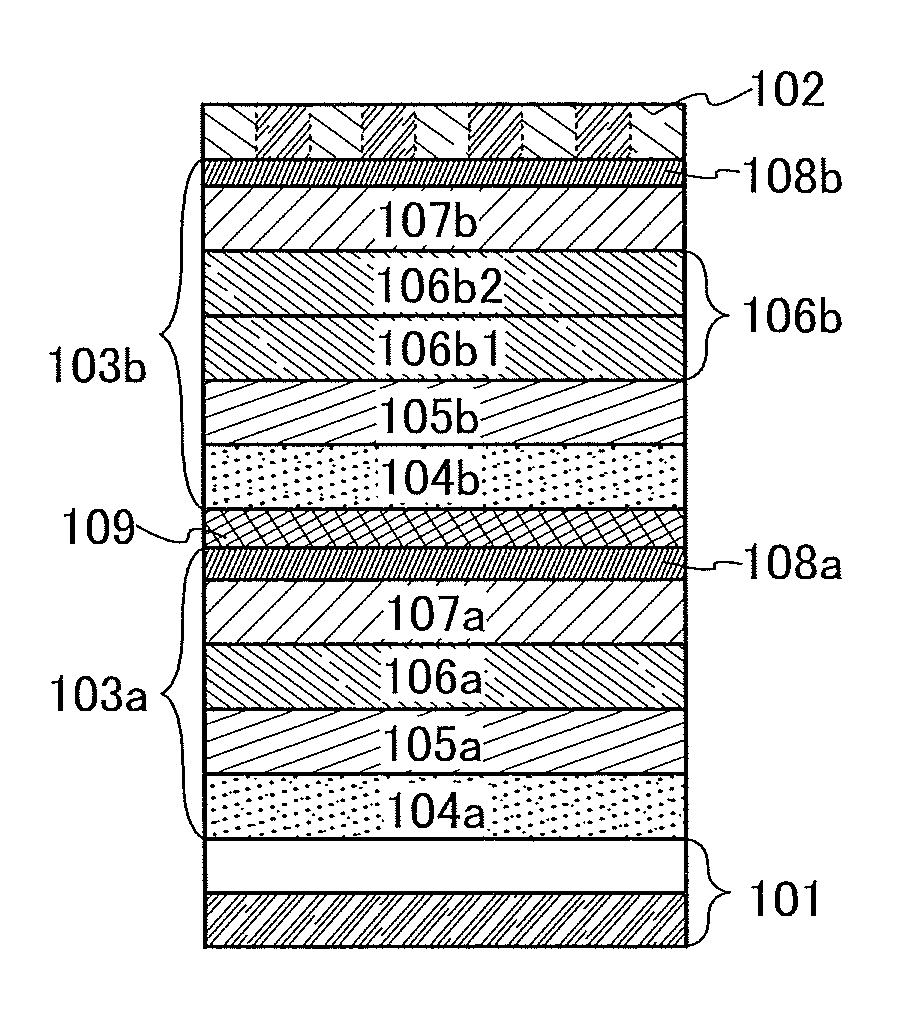
[0048]In this embodiment, a light-emitting element included in a light-emitting device that is one embodiment of the present invention is described.

[0049]The light-emitting element described in this embodiment has a structure in which an EL layer including a light-emitting layer is provided between a pair of electrodes. Note that a single EL layer may be included in the light-emitting element; alternatively, EL layers may be stacked with a charge generation layer provided therebetween (tandem structure). In this embodiment, a light-emitting element which has a tandem structure with two EL layers stacked is described with reference to FIG. 1.

[0050]The light-emitting element illustrated in FIG. 1 has a structure in which two EL layers (103a and 103b) each including a light-emitting layer are provided between a pair of electrodes (a first electrode 101 and a second electrode 102). In the EL layer 103a, a hole-injection layer 104a, a hole-transport layer 105a, a light-emitting layer 106...

embodiment 2

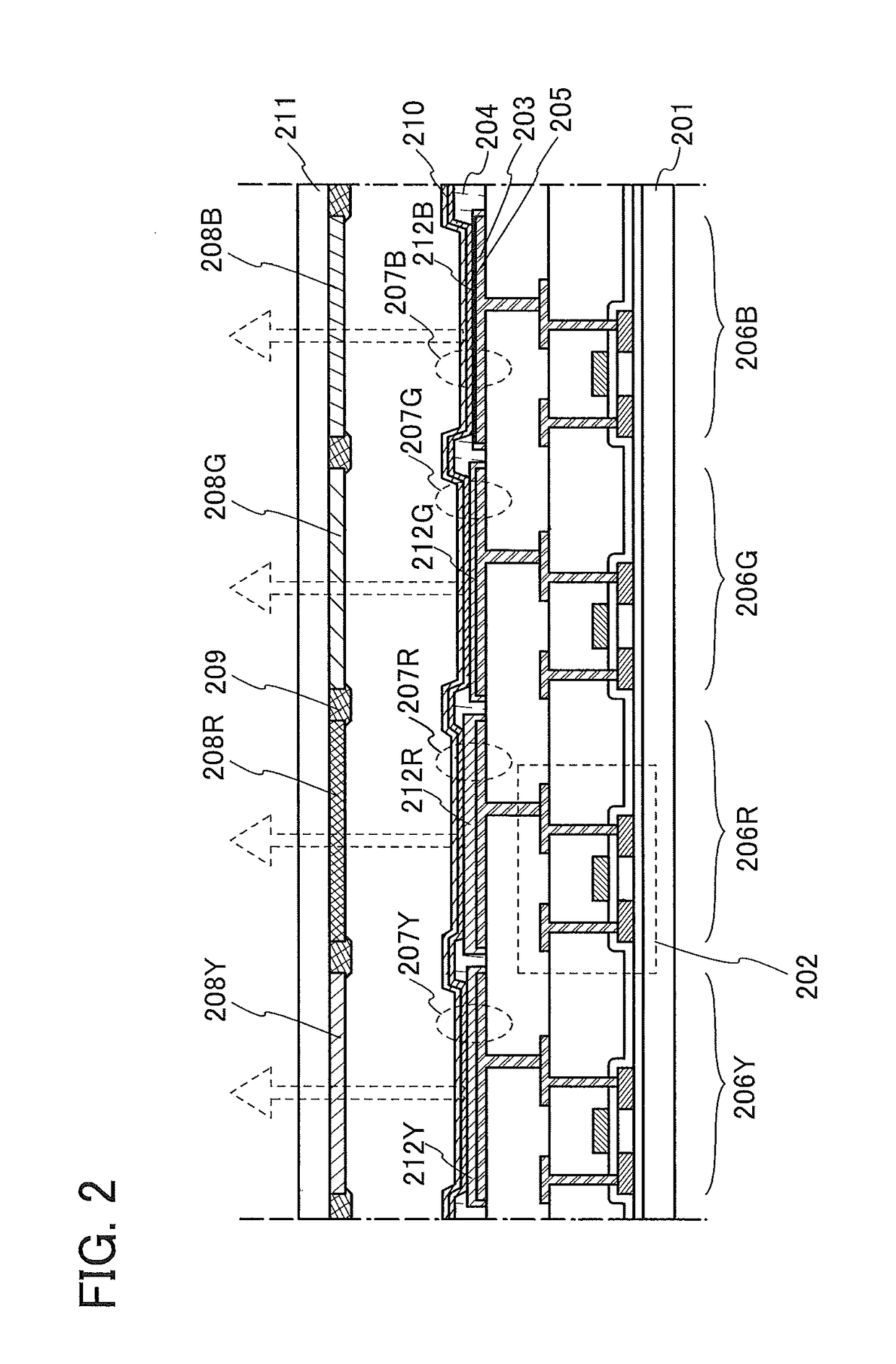
[0085]In this embodiment, one embodiment of a light-emitting device in which the light-emitting element described in Embodiment 1 is combined with a color filter or the like is described. In this embodiment, a structure of a pixel portion of the light-emitting device is described with reference to FIG. 2.

[0086]In FIG. 2, a plurality of FETs 202 is formed over a substrate 201. Each of the FETs 202 is electrically connected to a light-emitting element (207R, 207G, 207B, or 207Y). Specifically, each of the FETs 202 is electrically connected to a first electrode 203 that is a pixel electrode of a light-emitting element. A partition wall 204 is provided so as to cover edge portions of adjacent first electrodes 203.

[0087]The structure of the first electrode 203 in this embodiment is the same as that described in Embodiment 1 and the first electrode 203 serves as a reflective electrode. Conductive films (212B, 212G, 212R, and 212Y) which are transparent conductive films are formed as a par...

embodiment 3

[0093]In this embodiment, one embodiment of a light-emitting device in which the light-emitting element described in Embodiment 1 is combined with a color filter or the like is described. In this embodiment, a structure of a pixel portion of the light-emitting device is described with reference to FIG. 12.

[0094]In FIG. 12, a plurality of FETs 202 is formed over a substrate 201. Each of the FETs 202 is electrically connected to a light-emitting element (207R, 207G, 207B, or 207Y). Specifically, each of the FETs 202 is electrically connected to a first electrode 203 that is a pixel electrode of a light-emitting element. A partition wall 204 is provided so as to cover edge portions of adjacent first electrodes 203.

[0095]The structure of the first electrode 203 in this embodiment is the same as that described in Embodiment 1 and the first electrode 203 serves as a reflective electrode. Conductive films (212B, 212G, 212R, and 212Y) which are transparent conductive films are formed as a p...


PUM


Abstract

Provided is a light-emitting device which can emit monochromatic lights with high color purity due to a microcavity effect and which can provide a white light with a broad spectrum when the monochromatic lights are combined. The light-emitting device has a red-, green-, blue-, and yellow-emissive light-emitting elements each of which has a reflective electrode and a semi-transmissive and semi-reflective electrode. The red-, green-, blue-, and yellow-emissive light-emitting elements have the same structure other than the reflective electrode and a layer in contact with the reflective electrode to selectively emit red, green, blue, and yellow lights, respectively. Red, green, and blue color filters are also provided over the red-, green-, blue-, light-emitting elements, respectively. An EL layer is commonly shared by the red-, green-, blue-, and yellow-emissive light-emitting elements, and the semi-transmissive and semi-reflective electrode covers an edge portion of the EL layer.

Description

BACKGROUND OF THE INVENTION[0001]1. Field of the Invention[0002]One embodiment of the present invention relates to a light-emitting element in which an organic compound capable of providing light emission by application of an electric field is provided between a pair of electrodes, and also relates to a light-emitting device, an electronic device, and a lighting device including such a light-emitting element.[0003]Note that one embodiment of the present invention is not limited to the above technical field. Specifically, examples of the technical field of one embodiment of the present invention disclosed in this specification include a semiconductor device, a display device, a liquid crystal display device, a light-emitting device, a lighting device, a method for driving any of them, and a method for manufacturing any of them.[0004]2. Description of the Related Art[0005]As next generation lighting devices or display devices, display devices using light-emitting elements (organic EL ...

Claims


Application Information

Patent Timeline
Patent Type & Authority Patents(United States)
IPC IPC(8): H01L29/06H01L27/32H01L51/52
CPCH01L27/3213H01L51/5234H01L51/5265H10K59/351H10K50/828H10K50/852
Inventor SEO, SATOSHIOHSAWA, NOBUHARUSASAKI, TOSHIKI
Owner SEMICON ENERGY LAB CO LTD
Why Eureka
Try Eureka