
CMOS low voltage bandgap reference design with orthogonal output voltage trimming

a low-voltage bandgap and output voltage technology, applied in the field of semiconductor integrated circuits, can solve the problem that existing bvr circuit designs do not provide the necessary accuracy

Active Publication Date: 2017-07-04
SYNOPSYS INC
View PDF10 Cites 2 Cited by
  • Summary
  • Abstract
  • Description
  • Claims
  • Application Information

AI Technical Summary

Benefits of technology

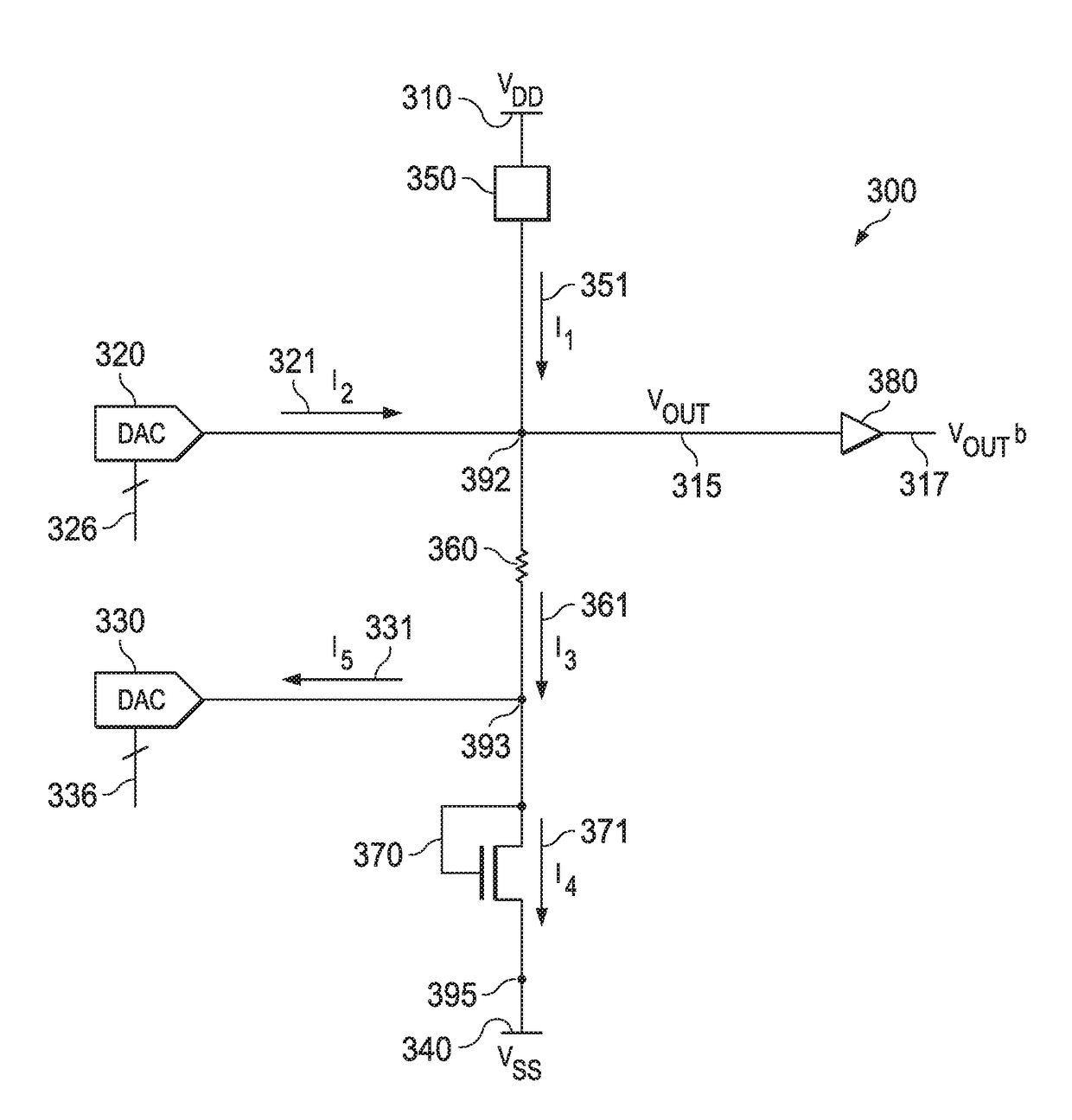
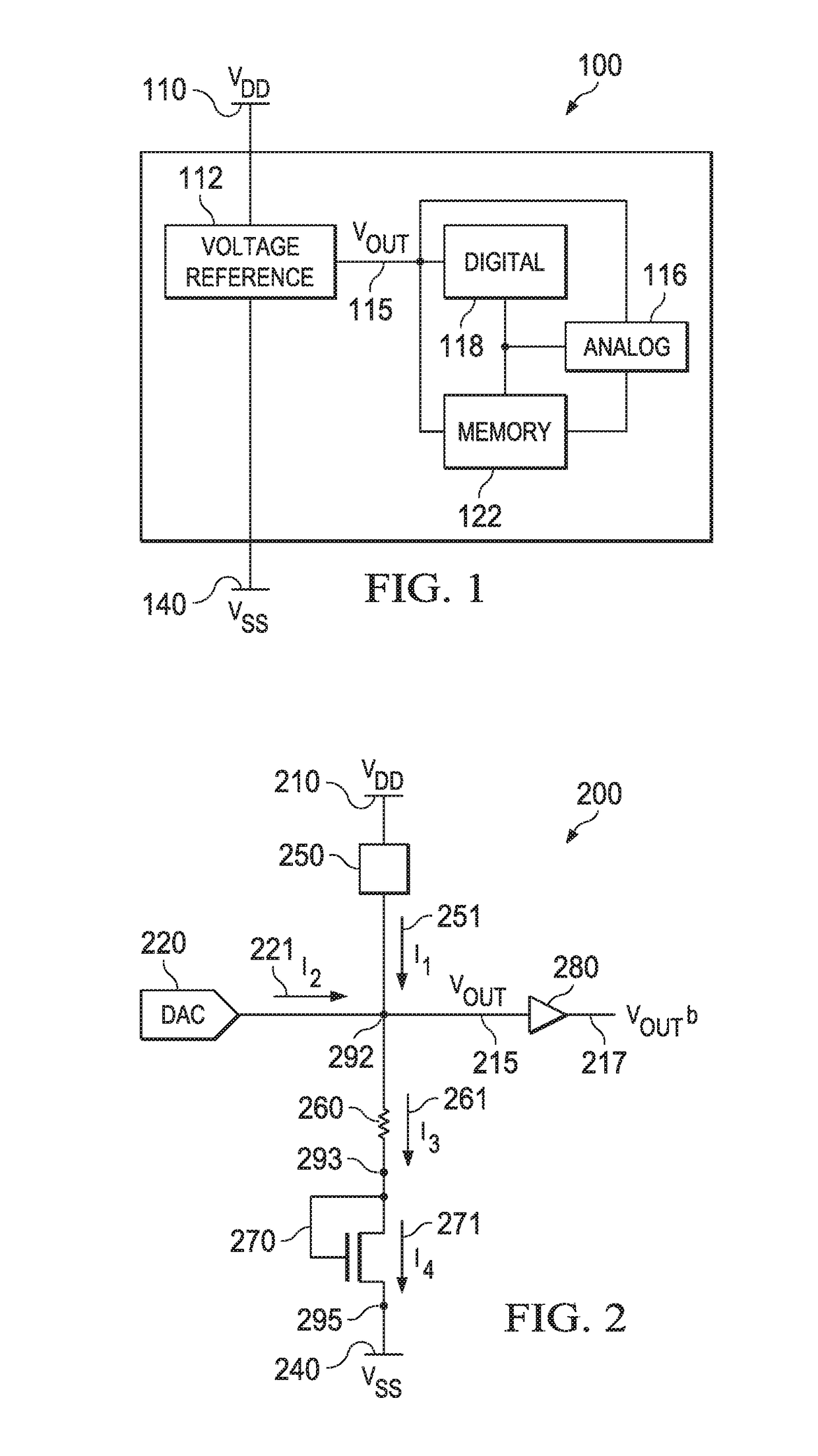
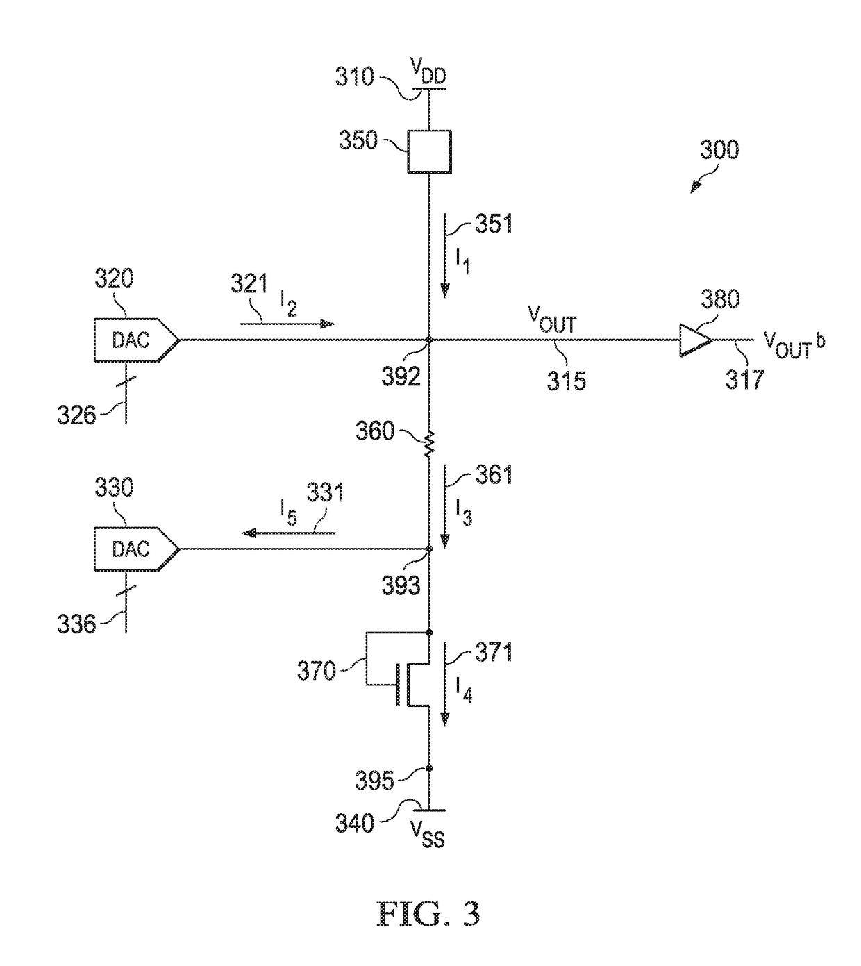
The patent describes a way to adjust the voltage of a low power circuit that produces a reference voltage. The voltage offset can be adjusted from a separate, temperature-independent current source, while the voltage temperature slope can be adjusted using a combination of two temperature-dependent current sources. These adjustments can help improve the accuracy and reliability of the reference voltage.

Problems solved by technology

However, existing BVR circuit designs do not provide necessary accuracy at the typical low core voltage associated with Fin Field Effect Transistors (FinFET) technology used in OTP and other low voltage transistor technology.

Method used


Image

  • CMOS low voltage bandgap reference design with orthogonal output voltage trimming
  • CMOS low voltage bandgap reference design with orthogonal output voltage trimming
  • CMOS low voltage bandgap reference design with orthogonal output voltage trimming

Examples


Embodiment Construction

[0008]In bandgap reference design, a precision voltage reference insensitive to process, supply voltage and temperature is obtained by summing a voltage that is proportional to absolute temperature (PTAT) and a voltage with negative temperature coefficient, which is complementary to absolute temperature (CTAT). In conventional BVR design, the CTAT voltage may be generated using a forward biased p-n junction having a temperature coefficient of −2 mV / ° C. at room temperature. The PTAT voltage may be generated from a voltage difference of similar p-n junctions ratioed by N. When a p-n junction is in forward bias, its current can be expressed as:

ID=ISeqVA / kT  (EQ. 1)

where k is the Boltzmann constant, q is the electron charge and T is the temperature, and VA is a voltage across the p-n junction. In some embodiments, a diode-connected metal-oxide-semiconductor field-effect transistor (MOSFET) may be used in place of the p-n junction and the VA term from equation (1) may be VGS, a gate-sou...


PUM


Abstract

Bandgap Voltage Reference circuits configured to produce reference voltages with both voltage offset and a voltage temperature slope are disclosed. By generating the voltage offset from a temperature-independent current, the voltage offset of the reference voltage may be temperature-independent, while generating the voltage temperature slope from a temperature-dependent current allows the voltage temperature slope to vary with temperature. To ensure that the voltage offset remains independent from the voltage temperature slope, an apparatus is disclosed for orthogonal trimming of voltage offset and voltage temperature slope.

Description

FIELD OF THE DISCLOSURE[0001]This disclosure relates generally to semiconductor integrated circuits, and more particularly to bandgap voltage reference circuits with programmable temperature slope and programmable voltage offset.BACKGROUND OF THE DISCLOSURE[0002]Very-large-scale-integration (VLSI) circuits require stable and predictable voltage references over PVT (Process, supply Voltage, and Temperature) variations. Bandgap Voltage Reference (BVR) circuits are used to produce these temperature-independent voltage references. Some One Time Programmable (OTP) non-volatile memory designs require BVR circuits to be powered with core voltage. However, existing BVR circuit designs do not provide necessary accuracy at the typical low core voltage associated with Fin Field Effect Transistors (FinFET) technology used in OTP and other low voltage transistor technology.SUMMARY OF THE DISCLOSURE[0003]An apparatus is provided for independently adjusting voltage offset and voltage temperature s...

Claims


Application Information

Patent Timeline
IPC IPC(8): G05F3/16G05F3/02H03K5/08
CPCG05F3/02H03K5/08
Inventor FANG, WEN
Owner SYNOPSYS INC
Learn More