Angular velocity sensor and manufacturing method therefor

a technology of angular velocity sensor and manufacturing method, which is applied in the direction of speed measurement using gyroscopic effects, instruments, surveying and navigation, etc., can solve the problems of increasing the cost of soi wafer, increasing the cost of the device, and difficulty in uniform thickness of the device layer

Active Publication Date: 2017-07-11
FUJIFILM CORP
View PDF18 Cites 6 Cited by
  • Summary
  • Abstract
  • Description
  • Claims
  • Application Information

AI Technical Summary

Benefits of technology

[0008]However, since the a SOI wafer is produced in a complex process of bonding two silicon (Si) substrates, polishing the silicon substrates, and thereby adjusting the thickness of the device layer, there is a problem that the SOI wafer requires considerably increased cost relative to a conventional Si wafer, causing increase in the device cost. In addition, when it is attempted to achieve further miniaturization of the device while maintaining a resonance frequency of the angular velocity sensor, it is necessary to reduce the dimension of the diaphragm diameter and at the same time reduce the thickness of the diaphragm.
[0050]According to the present invention, manufacturing is possible with cost lower than that of a conventional angular velocity sensor manufactured using an SOI substrate. In addition, according to the present invention, further miniaturization of the angular velocity sensor is possible, and deviation from the resonance frequency in design is maintained within an allowable range.

Problems solved by technology

However, since the a SOI wafer is produced in a complex process of bonding two silicon (Si) substrates, polishing the silicon substrates, and thereby adjusting the thickness of the device layer, there is a problem that the SOI wafer requires considerably increased cost relative to a conventional Si wafer, causing increase in the device cost.
However, in the process using the SOI wafer, due to the problem of polishing techniques, it is difficult to make the device layer thickness uniformly thin.
Since unevenness in the order of ±0.5 micrometer (μm) generally exists in the device layer thickness due to the limitation resulting from polishing accuracy, the unevenness of the film thickness increases by ±10% or more in response to the thickness of the device layer becoming 5 micrometers (μm) or less.
Since the thickness of the diaphragm considerably affects the resonance frequency, deviation (error) of the actual resonance frequency with reference to the design resonance frequency of the angular velocity sensor exceeds an allowable range in response to the unevenness of the film thickness becoming ±10% or more, making it difficult to realize practical mass production.
In other words, there are limits to miniaturization of the angular velocity sensor in the process using the conventional SOI wafer.

Method used


Image

  • Angular velocity sensor and manufacturing method therefor
  • Angular velocity sensor and manufacturing method therefor
  • Angular velocity sensor and manufacturing method therefor

Examples


example of application

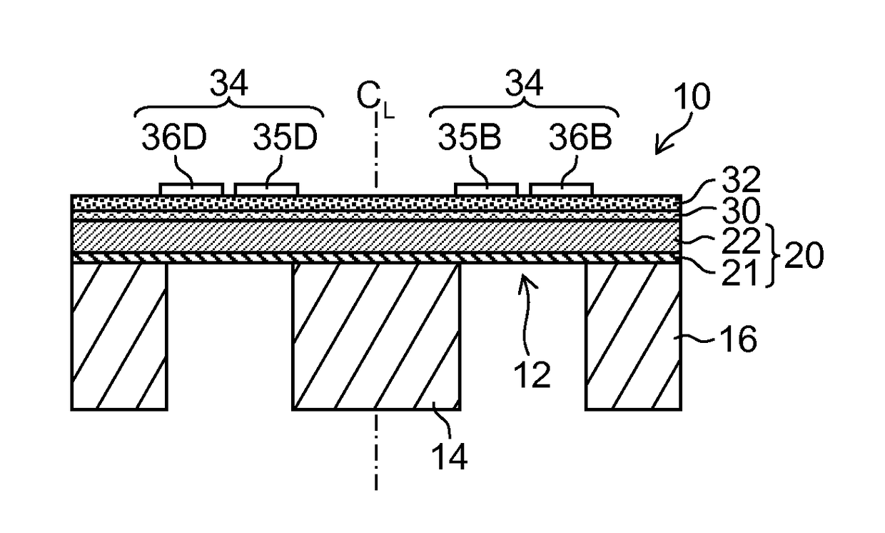
[0181]For example, in a case where an SOI wafer is used as a substrate, a device layer (Si-active layer) that becomes the principal part of a vibration plate is in principle in a state of no stress, but when residual stress of the piezoelectric-body film formed thereon is large, the value of resonance frequency is shifted relative to the design value, and it may occur that the specification value as a device is not satisfied.

[0182]In a case where the piezoelectric-body thin film is a PZT film, the film generally has a residual stress in a tensile direction. In this case, when a stress control layer is inserted as a layer constituting a vibration plate such that Teff calculated from the expression (7) is maintained within the range identified by the expression (15), the expression (16), or the expression (17), it is possible to suppress the amount of shift of resonance frequency within the allowable range.

[0183]As one example, it is contemplated that thermally oxidized SiO2 having a ...

modified example

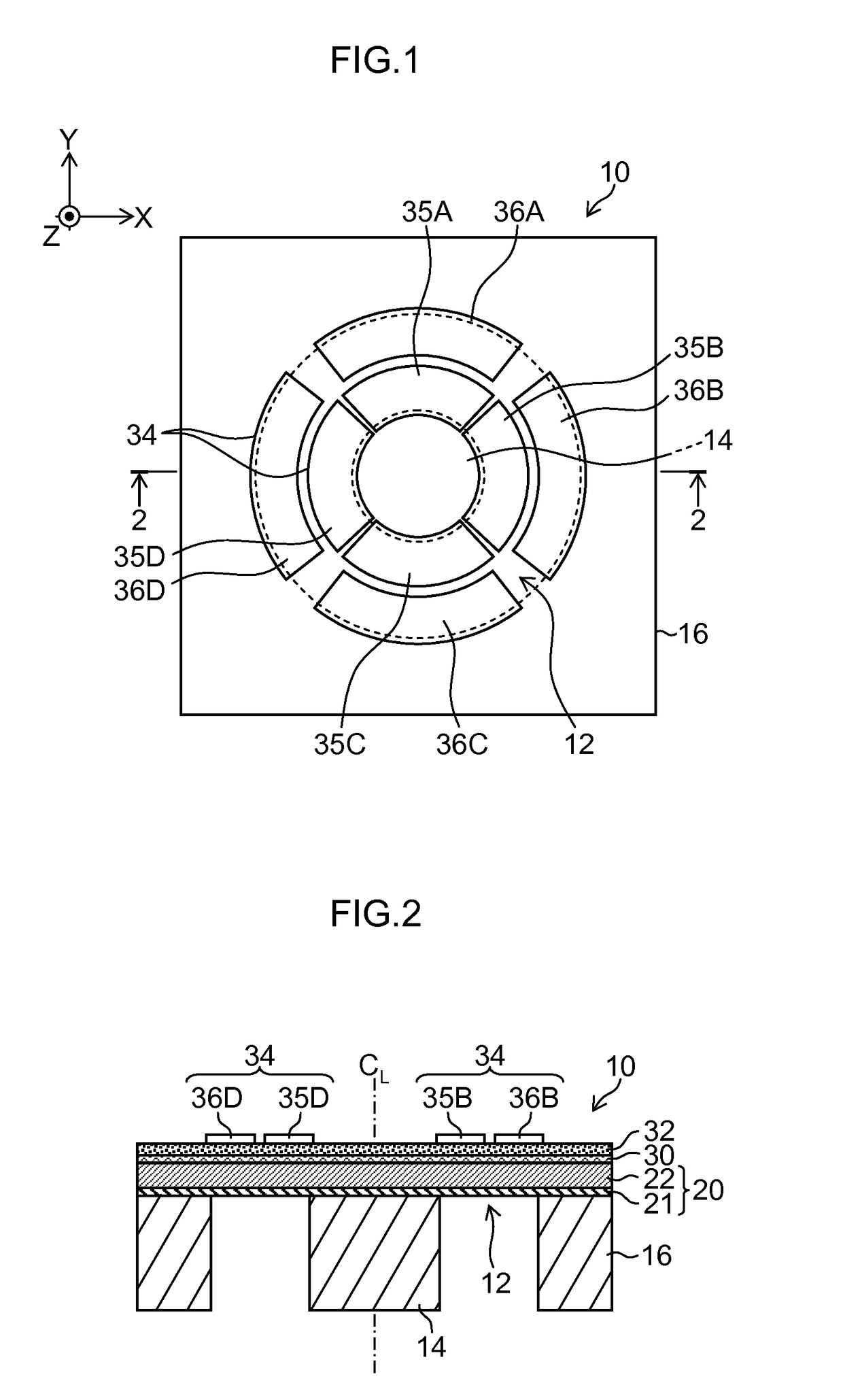
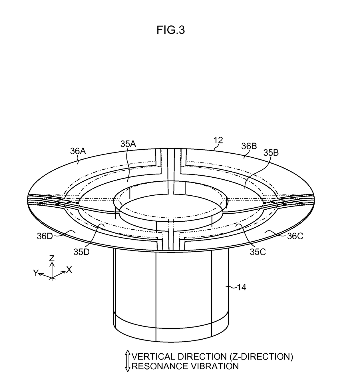
[0204]Although the diaphragm part that has the circular shape in a plan view has been described with reference to FIG. 1, but the shape is not limited to the circular shape and other configurations are possible such as a diaphragm part in an elliptical shape in a plan view and a diaphragm part in a polygonal shape in a plan view.


PUM


Abstract

One or more vibration plate layers of a diaphragm part are formed by a thin film forming technique. When a resonance frequency in a resonance vibration mode calculated from dimensions of a structure of an angular velocity sensor and an elastic parameter of a material thereof is defined as f kilohertz, a mass of a weight part is defined as M milligrams, a circumference of the diaphragm part is defined as r meters, a stress applied to a piezoelectric layer is defined as σp pascals, a thickness thereof is defined as tp meters, a stress applied to an n-th layer from the weight part in a vibration plate portion constituted by a plurality of layers including a lower electrode and the vibration plate layers is defined as σn pascals, and a thickness thereof is defined as tn meters (where n is a natural number), Teff expressed by Teff=r(σptp+Σσntn) / M satisfies {(−0.36f2+210) / 33}≦Teff≦{(0.44f2+210) / 33}.

Description

CROSS-REFERENCE TO RELATED APPLICATIONS[0001]This application is a continuation of PCT International Application No. PCT / JP2014 / 051929 filed on Jan. 29, 2014, which claims priority under 35 U.S.C. §119(a) to Japanese Patent Application No. 2013-019736 filed on Feb. 4, 2013. Each of the above applications is hereby expressly incorporated by reference, in their entirety, into the present application.BACKGROUND OF THE INVENTION[0002]Field of the Invention[0003]The present invention relates to an angular velocity sensor and a manufacturing method thereof, and in particular to an angular velocity sensor of a vibration gyro type having a structure in which a weight is supported by a piezoelectric diaphragm, and a manufacturing technique thereof.[0004]Description of the Related Art[0005]A MEMS (Micro Electro Mechanical System) vibrating gyrosensor using a silicon (Si) fine-processing technique has features such as being small in size and of low power consumption and various applications th...

Claims


Application Information

Patent Timeline
Patent Type & Authority Patents(United States)
IPC IPC(8): G01C19/56G01P15/09G01C19/5712G01P15/097G01C25/00
CPCG01C19/5712G01C19/56G01C25/00G01P15/09G01P15/097
Inventor NAONO, TAKAYUKINAKANO, TAKUMA
Owner FUJIFILM CORP
Why Eureka
Try Eureka