

Processing systems and methods for halide scavenging
a technology of halide scavenging and processing systems, applied in the direction of conveyor parts, transportation and packaging, coatings, etc., can solve the problems of local plasma damage to the substrate, wet process may have difficulty in penetrating some constrained, deformation of remaining materials, etc., to limit the aging defects of the substrate
- Summary
- Abstract
- Description
- Claims
- Application Information
AI Technical Summary
Benefits of technology
Problems solved by technology
Method used
Image

Examples
Embodiment Construction
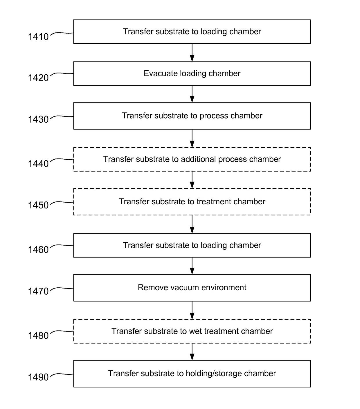
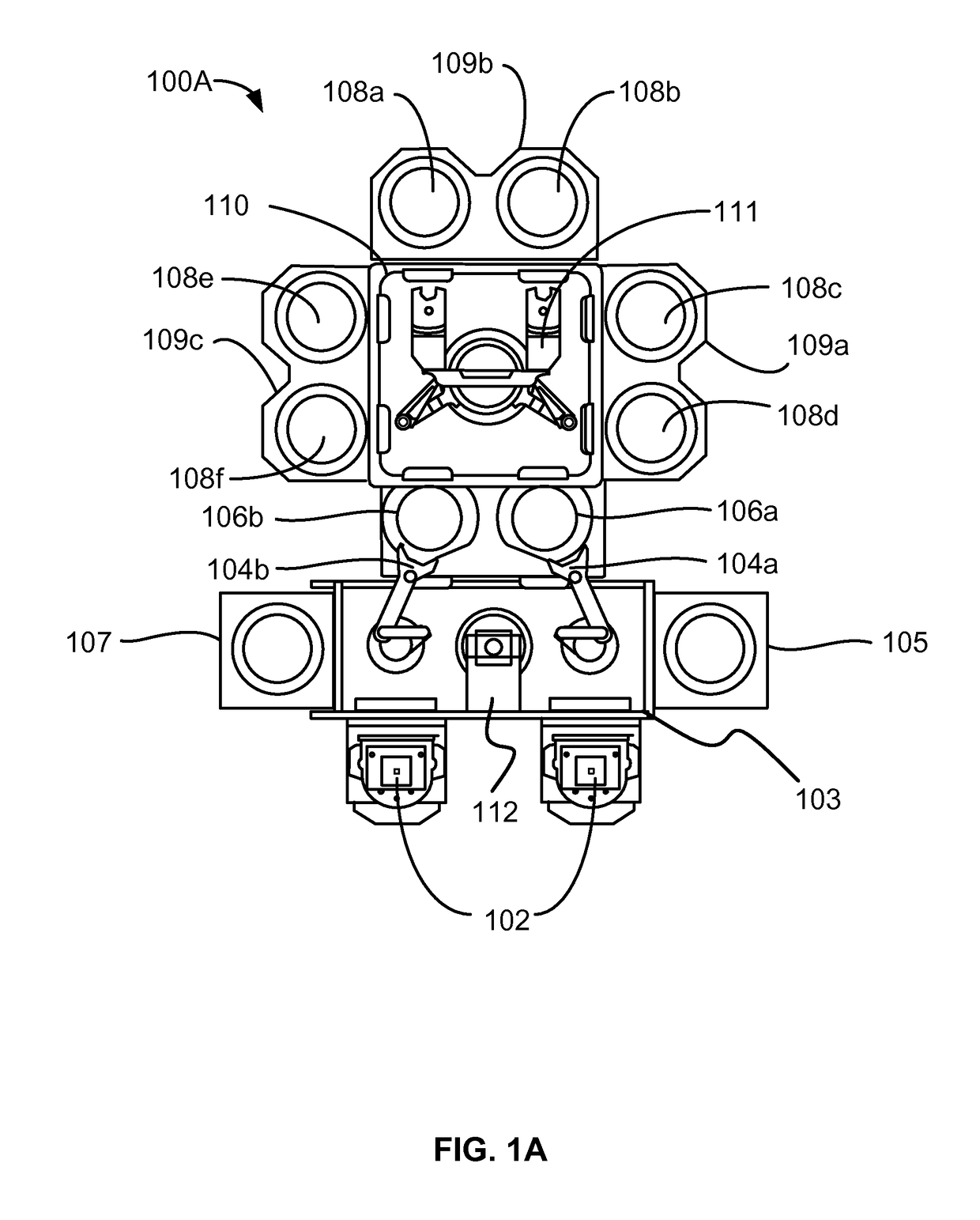
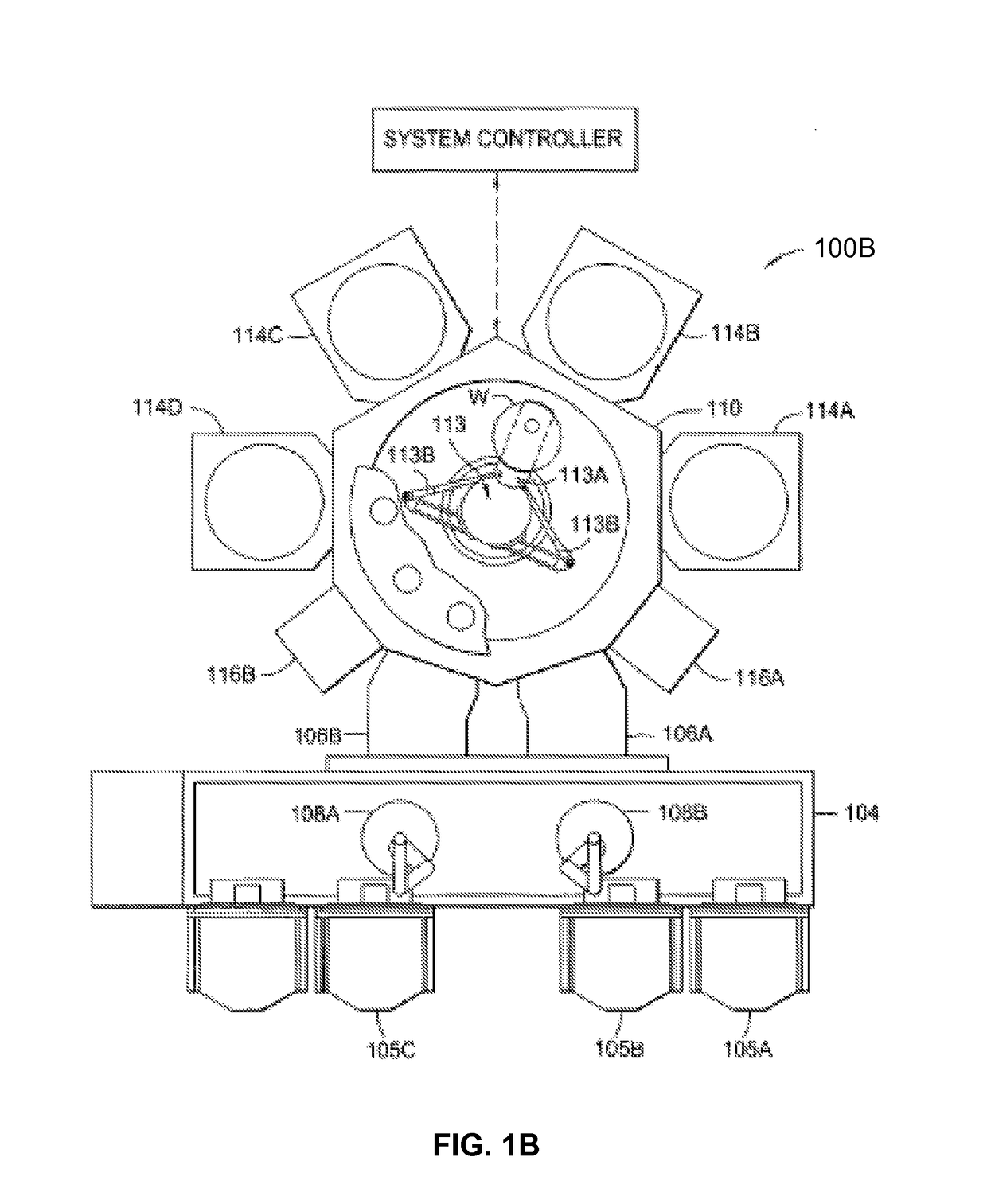
[0065]The present technology includes improved systems and methods for reducing halide contamination of semiconductor substrate films. The systems and methods also provide improved process structures to limit moisture interaction with processed substrates. Various dry etching processes utilize halide-containing precursors in the processes. When selective etch processes are performed, the non-selective material, or the material that is etched slower, or less, or not at all, may still be exposed to the precursors and chemicals used in the etch process. For example, certain etch processes that utilize radicalized fluorine-containing precursors are selective to silicon, silicon nitride, and various metals as compared to oxide materials. When the etch process is performed, the oxide material may still be exposed to the chemical etchants despite that the material is not removed. In certain scenarios, radical fluorine or other radical halides produced in the process may interact with and / o...
PUM
| Property | Measurement | Unit |
|---|---|---|
| Temperature | aaaaa | aaaaa |
| Temperature | aaaaa | aaaaa |
| Temperature | aaaaa | aaaaa |
Abstract
Description
Claims
Application Information