
Method for manufacturing semiconductor device, and semiconductor device

a manufacturing method and semiconductor technology, applied in the direction of lasers, laser optical resonator construction, laser details, etc., can solve the problems of increasing voltage, reducing product processing capability, and driving up manufacturing costs, so as to reduce electrode surface area, less side etching, and less voltage attributable

Active Publication Date: 2017-07-11
NICHIA CORP
View PDF16 Cites 0 Cited by
  • Summary
  • Abstract
  • Description
  • Claims
  • Application Information

AI Technical Summary

Benefits of technology

This approach effectively reduces side etching and maintains proper electrode surface area, suppressing voltage increases by controlling the etching process through multiple mask layers and techniques, enhancing semiconductor device performance.

Problems solved by technology

Fine working is possible by using dry etching, which allows ion etching and other such anisotropic etching, but this entails the installation of large equipment decreases product processing capability, so it drives up the manufacturing cost.
In the case where side etching proceeds in the formation of an electrode, there will be a reduction in the contact surface area, and this may result in the problem of a voltage increase.

Method used


Image

  • Method for manufacturing semiconductor device, and semiconductor device
  • Method for manufacturing semiconductor device, and semiconductor device
  • Method for manufacturing semiconductor device, and semiconductor device

Examples


embodiment 1

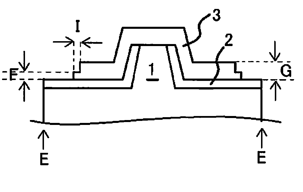
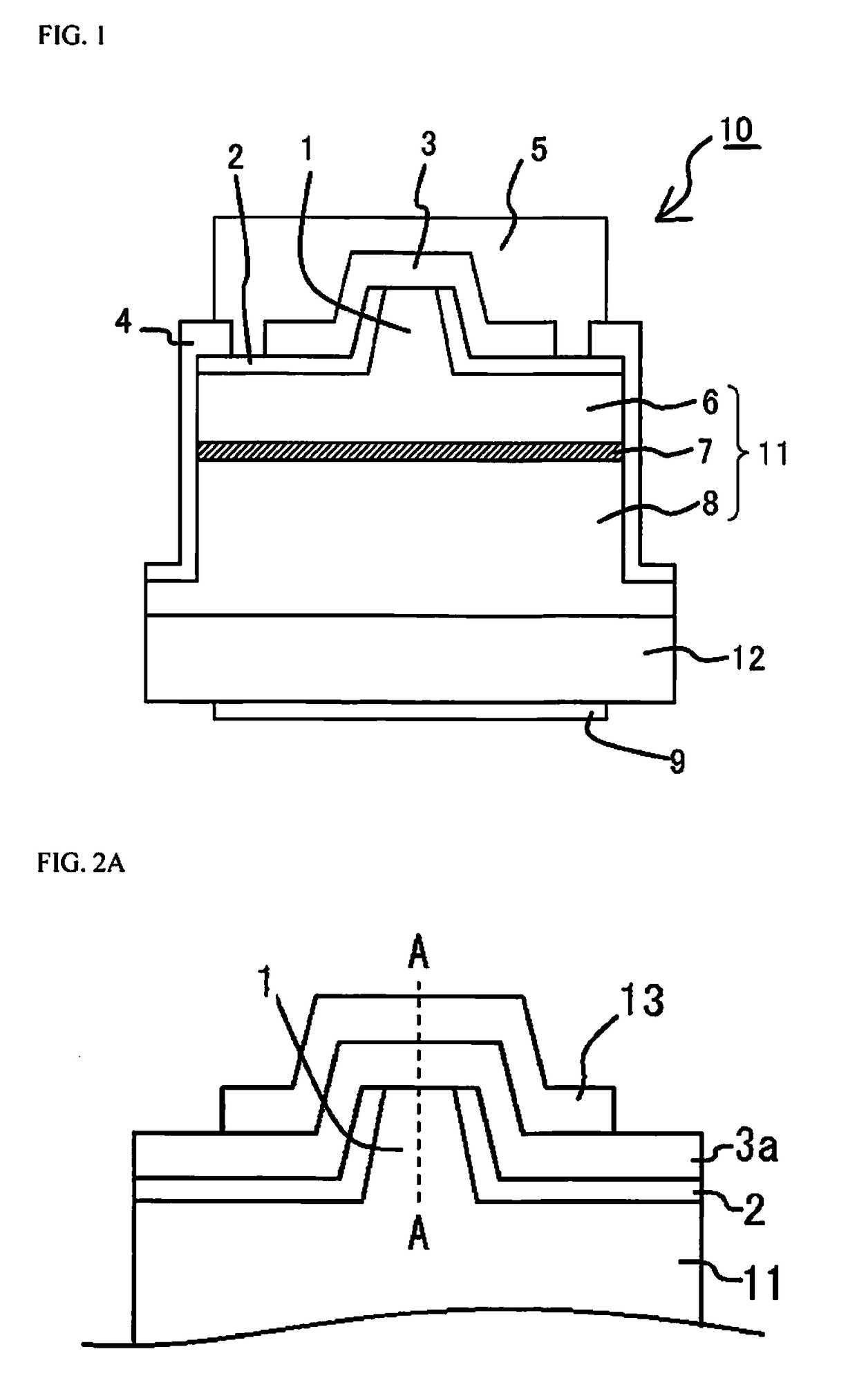
[0087]In this embodiment, the semiconductor device is the laser device 10 shown in FIG. 1, and primarily has a semiconductor layer 11 and a p electrode 3 formed on a main face of the semiconductor layer 11.

[0088]The semiconductor layer 11 has a rectangular shape in plan view, measuring about 200×800 μm. The semiconductor layer 11 is usually formed on a substrate that is a few inches in diameter, after which the electrodes and so forth are formed, and these are then separated into individual rectangular laser devices. Prior to this separation, the imaginary lines indicating the expected positions for division into individual units are planned division lines, which include a planned division line extending parallel to the first direction (M in FIG. 7C), and a planned division line extending in a direction that intersects (typically, one that is perpendicular to) the first direction.

[0089]The semiconductor layer 11 consists of an n-type semiconductor layer 8, an active layer 7, and a p...

embodiment 2

[0106]As shown in FIG. 5, in the method for manufacturing a laser device in Embodiment 1, the second mask 14 is formed without removing the first mask 13, the third mask 16 is formed without removing these first two masks, and etching is performed using the resulting masks sequentially.

[0107]Other than this, the manufacturing method is similar to in Embodiment 1, and has a similar effect to Embodiment 1.

[0108]In particular, laminating the first to third masks simplifies the work entailed by the process.

embodiment 3

[0109]As shown in FIG. 6, in the method for manufacturing a laser device in Embodiment 1, a second mask 24 that is larger in the desired location is formed on the first mask 13, and second etching is performed.

[0110]Other than this, the manufacturing method is similar to in Embodiment 1, and has a similar effect to Embodiment 1.

[0111]In particular, putting the second mask in the desired shape allows the conventional pattern shape to be maintained.


PUM


Abstract

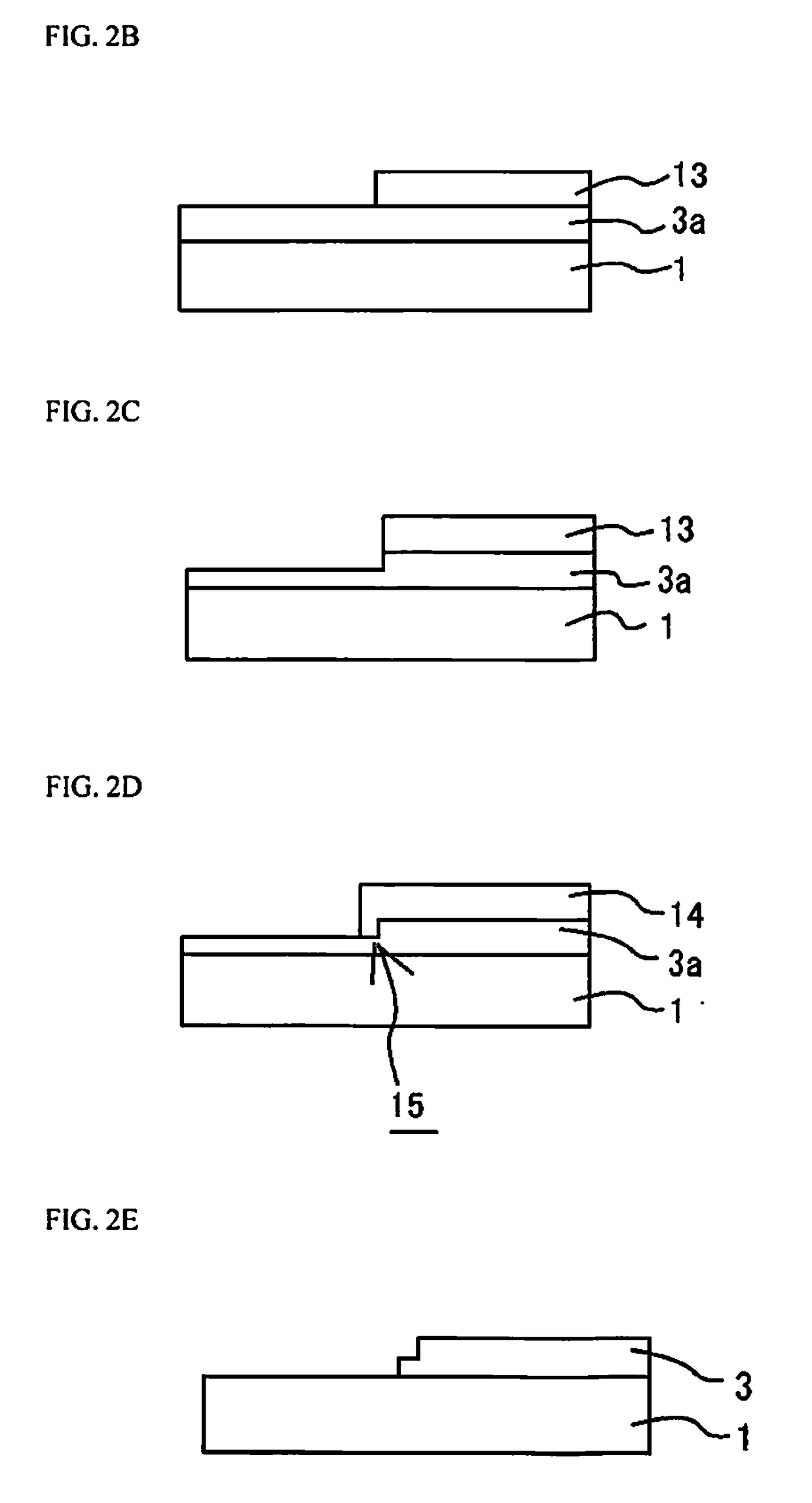
With a method for manufacturing a semiconductor device, a semiconductor layer having a protrusion on a main face is formed. The protrusion includes an upper face and side faces. A conductive layer on a region that includes at least the upper face and the side faces of the protrusion is formed. A first mask that partially covers a surface of the conductive layer is formed. A part of the conductive layer is etched by using the first mask in a first etching process. A second mask that at least partially covers the surface of the conductive layer that has undergone the first etching process is formed. A part of the conductive layer is etched by using the second mask to expose a part of the semiconductor layer and to form the conductive layer into an electrode in a second etching process.

Description

CROSS-REFERENCE TO RELATED APPLICATIONS[0001]This application claims priority to Japanese Patent Application No. 2015-033172 filed on Feb. 23, 2015. The entire disclosure of Japanese Patent Application No. 2015-033172 is hereby incorporated herein by reference.BACKGROUND[0002]1. Technical Field[0003]The present disclosure relates to a method for manufacturing a semiconductor device, and to a semiconductor device.[0004]2. Description of Related Art[0005]A method that was commonly known in the past when a metal film was formed as a pattern in a semiconductor manufacturing process involved forming a resist on the layer to be worked, patterning the resist by exposure to light to create a mask, and dissolving the worked layer with a chemical etching solution to form a pattern. It has been proposed with this method, for example, that the amount of side etching can be reduced by increasing adhesion between the resist and the worked layer (for example, JPH5-13401A).[0006]It has also been pr...

Claims


Application Information

Patent Timeline
Patent Type & Authority Patents(United States)
IPC IPC(8): H01S5/22H01S5/10H01S5/20H01S5/343H01S5/16
CPCH01S5/22H01S5/1017H01S5/16H01S5/2081H01S5/2214H01S5/34333
Inventor HARADA, SUSUMU
Owner NICHIA CORP
Learn More