Integrated photo detector, method of making the same

a photo detector and integrated technology, applied in the direction of instruments, optical elements, optical waveguide light guides, etc., can solve the problems of large bandwidth, limited popular applications, and inability to protect the integrated photodiode, so as to improve the esd protection capability and enhance the esd protection, no impact on the high-speed performance of ge pd

Active Publication Date: 2017-08-08
MARVELL ASIA PTE LTD
View PDF4 Cites 16 Cited by
  • Summary
  • Abstract
  • Description
  • Claims
  • Application Information

AI Technical Summary

Benefits of technology

[0008]In another specific embodiment, the present invention provides an integrated photo detector with enhanced electrostatic discharge damage (ESD) protection. The integrated photo detector includes a Germanium photodiode comprising an intrinsic Germanium layer formed on a p-type Silicon base layer patterned within a Si-on-Insulator (SOI) substrate. The intrinsic Germanium layer includes a first n++ doped region and the p-type Silicon base layer comprising a first p++ doped region. Additionally, the integrated photo detector includes a Silicon photodiode comprising a Silicon region patterned within the SOI substrate to form a p-type Silicon portion joined with a n-type Silicon portion. The p-type Silicon portion includes a second p++ doped region and the n-type Silicon portion comprising a second n++ doped region. Furthermore, the integrated photo detector includes a first metallic layer being pattered to include a first p-electrode coupled to the first p++ doped region, a second p-electrode coupled to the second p++ doped region, a first electrode connected to the first p-electrode by a portion of the first metallic layer with a reducing width and connected to the second p-electrode by a first trace line. Moreover, the integrated photo detector includes a second metallic layer being pattered to include a first n-electrode coupled to the first n++ doped region, a second n-electrode coupled to the second n++ doped region, a second electrode connected to the first n-electrode by a portion of the second metallic layer with a reducing width and connected to the second n-electrode by a second trace line. The Silicon photodiode is coupled with the Germanium photodiode electrically in parallel with a capacitance of no greater than a few femto Faradays and an enhanced ESD threshold of about ±100V.
[0010]Many benefits can be achieved with the present invention based on integrating Ge PD with a Si PD in parallel on the same substrate. The higher ESD threshold of the added Si PD helps to improve the ESD protection capability of the integrated photodiode. The small capacitance introduced by the added Si PD, which is in a few femto Faradays range and is several orders of magnitudes lower than that of a conventional Zener diode for ESD protection, the enhanced ESD protection by the added Si PD causes no impact on the high-speed performance of Ge PD. Additionally, Si-based and Ge-based PN junction photo diode can be easily fabricated on SOI substrate in a unified process to form various integrated silicon photonics circuits.

Problems solved by technology

In the early days Internet, popular applications were limited to emails, bulletin board, and mostly informational and text-based web page surfing, and the amount of data transferred was usually relatively small.
Today, Internet and mobile applications demand a huge amount of bandwidth for transferring photo, video, music, and other multimedia files.
The communication transmission or reception using the traditional cable is limited to bandwidth and transmission speed of the traditional cable and mass information transmission required in modern life causes the traditional communication replaces the traditional communication transmission system gradually for systems requiring higher bandwidth and longer distance that electrical cable cannot accommodate.
However, high-speed Ge photodiode is vulnerable to electrostatic discharge damage (ESD).
Because of its low ESD threshold, many silicon photonics communication modules having Ge photo detectors suffered low assembly yield.
Typically, for providing ESD protection purpose, the Zener diode chip is formed separately and mounted or connected to a photodiode chip by solder bump or wire bonding, making the silicon photonics integration level much lower and vulnerable to reliability and assembly yield issue.

Method used


Image

  • Integrated photo detector, method of making the same
  • Integrated photo detector, method of making the same
  • Integrated photo detector, method of making the same

Examples


Embodiment Construction

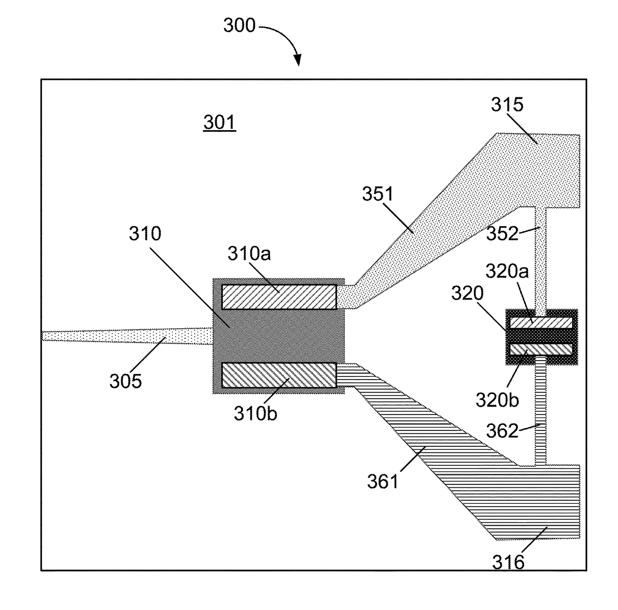
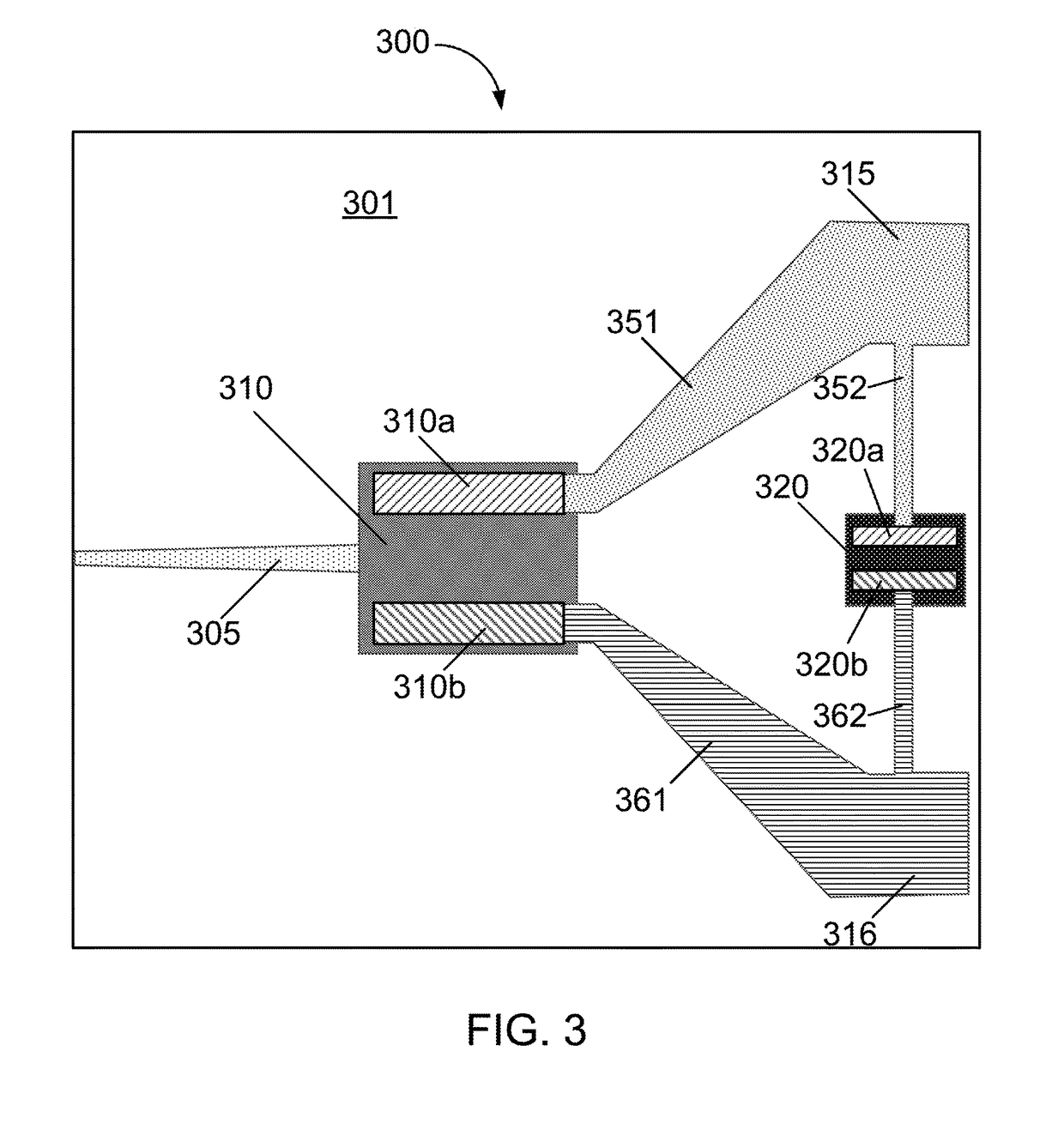
[0021]The present invention relates to a high-speed optic-electric telecommunication device. More particularly, the present invention provides an integrated photo detector with improved electrostatic discharge damage threshold and a method of making the same. Merely by example, the present invention discloses an integrated photo detector and a method for forming the same by coupling a Si photodiode with a Ge photodiode in parallel fabricated on a same SOI substrate with an ESD threshold of about 100V for high-speed data communication, though other applications are possible.

[0022]The following description is presented to enable one of ordinary skill in the art to make and use the invention and to incorporate it in the context of particular applications. Various modifications, as well as a variety of uses in different applications will be readily apparent to those skilled in the art, and the general principles defined herein may be applied to a wide range of embodiments. Thus, the pre...


PUM


Abstract

An integrated photo detector with enhanced electrostatic discharge damage (ESD) protection. The integrated photo detector includes a first photodiode formed in the SOI substrate and associated with a first p-electrode and a first n-electrode. Additionally, the integrated photo detector includes a second photodiode formed in the SOI substrate associated with a second p-electrode and a second n-electrode forming a capacitance no larger than a few femto Faradays. Moreover, the integrated photo detector includes a first electrode and a second electrode disposed respectively on the SOI substrate. The first / second electrode is respectively connected to the first p / n-electrode via a first / second metallic layer patterned with a reduced width from the first / second electrode to the first p / n-electrode and connected to the second p / n-electrode via a first / second metallic wire to make a parallel coupling between the first photodiode and the second photodiode with an ESD threshold of about 100V.

Description

BACKGROUND OF THE INVENTION[0001]The present invention relates to a high-speed optic-electric telecommunication device. More particularly, the present invention provides an integrated photo detector with improved electrostatic discharge damage threshold and a method of making the same.[0002]Over the last few decades, the use of broadband communication networks exploded. In the early days Internet, popular applications were limited to emails, bulletin board, and mostly informational and text-based web page surfing, and the amount of data transferred was usually relatively small. Today, Internet and mobile applications demand a huge amount of bandwidth for transferring photo, video, music, and other multimedia files. For example, a social network like Facebook processes more than 500 TB of data daily. With such high demands on data and data transfer, existing data communication systems need to be improved to address these needs.[0003]As science and technology are updated rapidly, proc...

Claims


Application Information

Patent Timeline
Patent Type & Authority Patents(United States)
IPC IPC(8): G02B6/12H01L31/0232G02B6/42H01L31/02H01L31/18H01L31/028H01L27/02H01L31/0224
CPCG02B6/4275H01L31/02325H01L31/028H01L31/02019H01L27/0248H01L31/022408H01L31/1804H01L31/1808G02B6/12004G02B6/12G02B2006/12123H01L27/1443H01L31/02005H01L31/02327H01L31/103
Inventor LIN, JIEKATO, MASAKI
Owner MARVELL ASIA PTE LTD
Why Eureka
Try Eureka