Micromechanical component with a reduced contact surface and its fabrication method

a micromechanical and contact surface technology, applied in the field of micromechanical components with a reduced contact surface, can solve the problems of unsatisfactory vertical etches b>5/b>, and achieve the effect of improving the tribology of components

Active Publication Date: 2017-08-15
NIVAROX FAR
View PDF12 Cites 2 Cited by
  • Summary
  • Abstract
  • Description
  • Claims
  • Application Information

AI Technical Summary

Benefits of technology

[0008]It is an object of the present invention to overcome all or part of the aforecited drawbacks by proposing a new type of micromechanical component and a new type of fabrication method making it possible to improve the tribology of components formed by micromachining a wafer of material.
[0016]It is understood that two distinct types of etch are obtained in the same etching chamber. It is immediately clear that the oblique etch of step e) can form a substantially oblique second surface and form several micromechanical components on the same substrate having a peripheral wall with a reduced contact surface. It can also be observed that, as a result of the protective layer provided only on the vertical walls, the oblique etch of step e) allows for a considerably more open angle and a substantially rectilinear direction of etching, which avoids being limited by the parameters of a Bosch deep reactive ion etching which, conversely, is used in step c) with its optimised vertical etching parameters.
[0021]in step e), the continuous etching and passivation gas flows are pulsed to enhance the etch of the cavity bottom.
[0023]Advantageously according to the invention, it is understood that the peripheral or internal vertical wall of the micromechanical component offers a reduced contact surface or, on insertion of a member along an internal wall of the micromechanical component, can provide improved tribological contact with another component.

Problems solved by technology

After several years of fabrication, it was found that these vertical etches 5 were not entirely satisfactory, particularly as regards tribology.

Method used


Image

  • Micromechanical component with a reduced contact surface and its fabrication method
  • Micromechanical component with a reduced contact surface and its fabrication method
  • Micromechanical component with a reduced contact surface and its fabrication method

Examples


Embodiment Construction

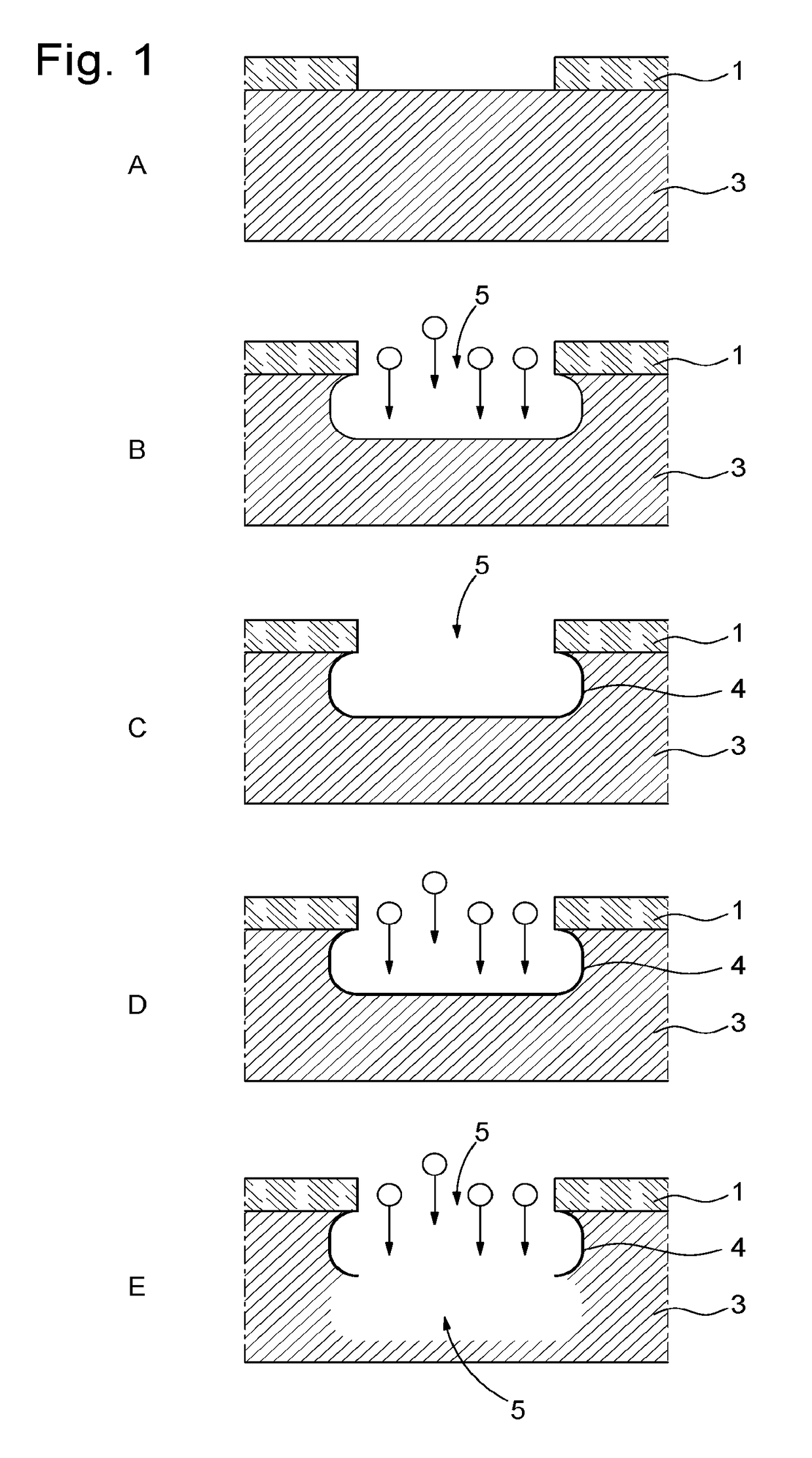
[0032]The invention relates to a method 11 for fabricating a silicon-based micromechanical component. As illustrated in FIG. 12, method 11 includes a first step 13 of taking a silicon-based substrate.

[0033]The term “silicon-based” means a material including single crystal silicon, doped single crystal silicon, polycrystalline silicon, doped polycrystalline silicon, porous silicon, silicon oxide, quartz, silica, silicon nitride or silicon carbide. Of course, when the silicon-based material is in crystalline phase, any crystalline orientation may be used.

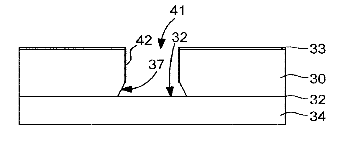
[0034]Typically, as illustrated in FIG. 4, the silicon-based substrate 31 may be a silicon-on-insulator substrate (also known by the abbreviation “SOI”) comprising an upper silicon layer 30 and a lower silicon layer 34 joined by an intermediate silicon oxide layer 32. However, alternatively, the substrate could comprise a silicon layer added to another type of base such as, for example, a metal base.

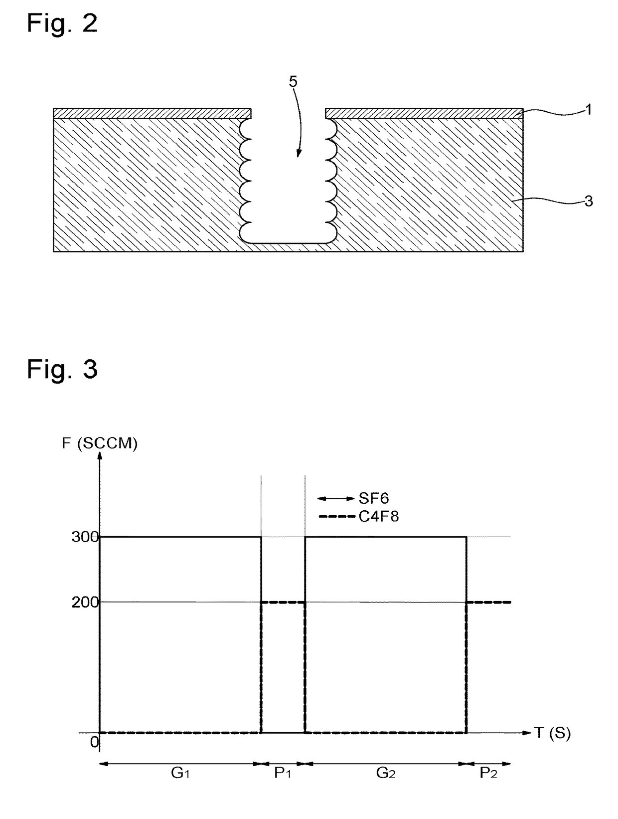
[0035]The method continues with ste...


PUM

PropertyMeasurementUnit
opening angleaaaaaaaaaa
open angleaaaaaaaaaa

Abstract

The invention relates to a silicon-based component with at least one reduced contact surface which, formed from a method combining at least one oblique side wall etching step with a “Bosch” etch of vertical side walls, improves, in particular, the tribology of components formed by micromachining a silicon-based wafer.

Description

[0001]This application claims priority from European Patent Application No. 15173825.9 filed on Jun. 25, 2015, the entire disclosure of which is hereby incorporated by reference.FIELD OF THE INVENTION[0002]The invention relates to micromechanical component with a reduced contact surface and a method for fabrication of the same. More specifically, the invention relates to such a component formed by micromachining a wafer of material.BACKGROUND OF THE INVENTION[0003]CH Patent 698837 discloses the fabrication of a timepiece component by micromachining a water of amorphous or crystalline material, such as crystalline or polycrystalline silicon.[0004]Such micromachining is generally obtained by deep reactive ion etching (also known by the abbreviation “DRIE”). As illustrated in FIGS. 1 to 3, a known micromachining method consists in structuring a mask 1 on a substrate 3 (cf. FIG. 1, step A) followed by a “Bosch” deep reactive ion etching combining in succession an etching phase (cf. FIG....

Claims


Application Information

Patent Timeline
Patent Type & Authority Patents(United States)
IPC IPC(8): B81C1/00G04B13/02G04D99/00
CPCB81C1/00619B81C1/00103G04B13/026G04D99/00B81B2201/035B81B2203/0384B81C2201/014B81C2201/0112B81C2201/0132B81C2201/0138B81C2201/0188B81C2201/0198B81B7/0032B81B7/0074B81C1/00B81C1/00388G04B13/02G04B13/027
Inventor GANDELHMAN, ALEXPIN, ANDRE
Owner NIVAROX FAR
Why Eureka
Try Eureka