Electronic apparatus and method for manufacturing the same

a technology of electronic equipment and flexible substrate, which is applied in the direction of non-linear optics, instruments, transportation and packaging, etc., can solve the problems of high rigidity of current used process, high cost of laser system, and difficulty in forming display units thereon, etc., and achieves simple and cheap

Active Publication Date: 2017-11-28
INNOLUX CORP
View PDF5 Cites 0 Cited by
  • Summary
  • Abstract
  • Description
  • Claims
  • Application Information

AI Technical Summary

Benefits of technology

[0011]Another object of the present invention is to provide a method for manufacturing an electronic apparatus, which can be used to produce a light and thin electronic apparatus on the current used machine.
[0041]In addition, when the method of the present invention is used to manufacture an electronic apparatus, it is not necessary to pattern the debonding layer, so the problem that the debonding layer cannot well adhered on the substrate or the carrier can be prevented. Furthermore, compared to the method using laser with single wavelength, the wavelength of the radiation using in the method of the present invention can be selected according to the light absorbing group of the material used in the debonding layer. Hence, the machine for the radiation can be varied, and not limited to the expansive laser system. Therefore, the method of the present invention can be used to prepare an electronic apparatus with a flexible substrate in a simple and cheap way.

Problems solved by technology

However, when the flexible substrate is a thin glass substrate having a thickness of 0.3 mm or less or a plastic substrate, the rigidity thereof is not high enough for the current used process.
Therefore, it is hard to form display units thereon through the current used process for manufacturing the display panel.
However, the laser system is expensive, the selection of suitable wavelength is less, and the time for performing the laser process is long.
Sometimes, the active units may be damaged, and the flexible plastic substrate may be yellowed and even carbonated when the energy of the laser is too high, resulting in the yield rate of the electronic products lowered.

Method used


Image

  • Electronic apparatus and method for manufacturing the same
  • Electronic apparatus and method for manufacturing the same
  • Electronic apparatus and method for manufacturing the same

Examples


Embodiment Construction

[0093]The present invention has been described in an illustrative manner, and it is to be understood that the terminology used is intended to be in the nature of description rather than of limitation. Many modifications and variations of the present invention are possible in light of the above teachings. Therefore, it is to be understood that within the scope of the appended claims, the invention may be practiced otherwise than as specifically described.

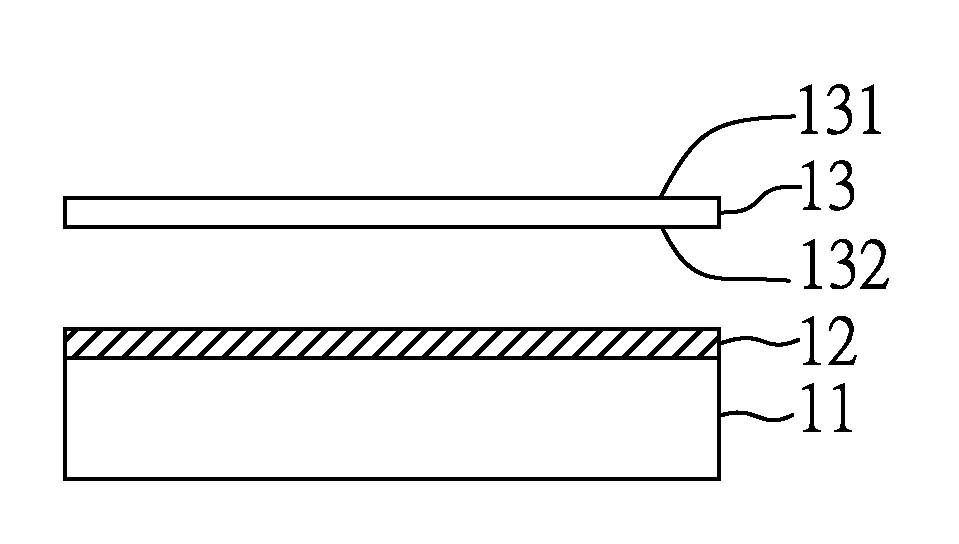
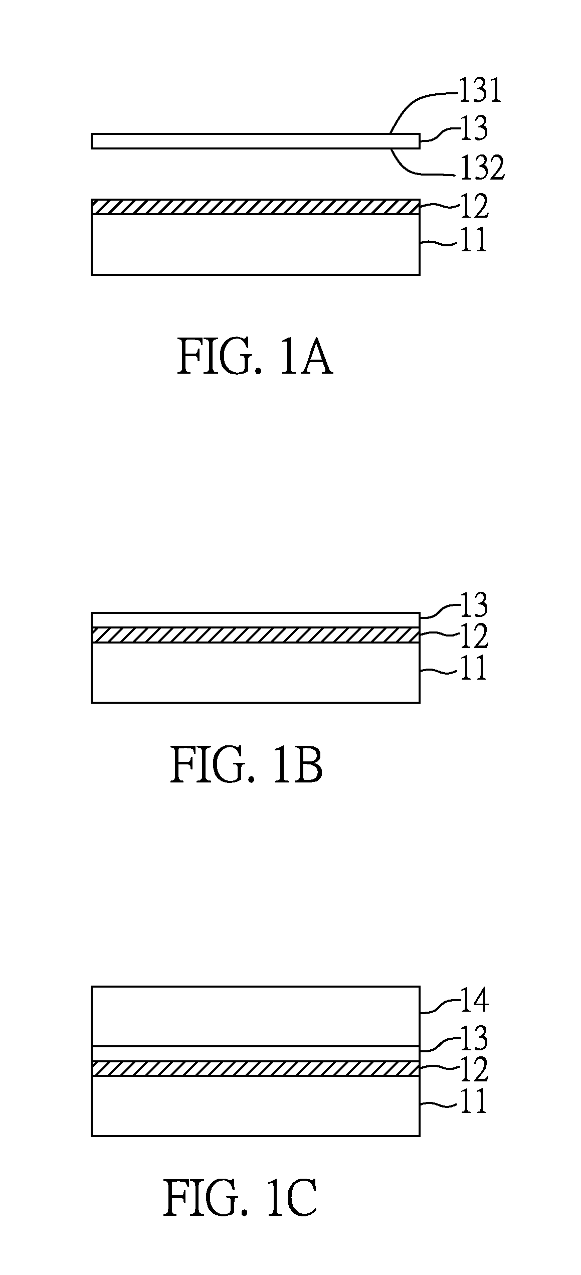
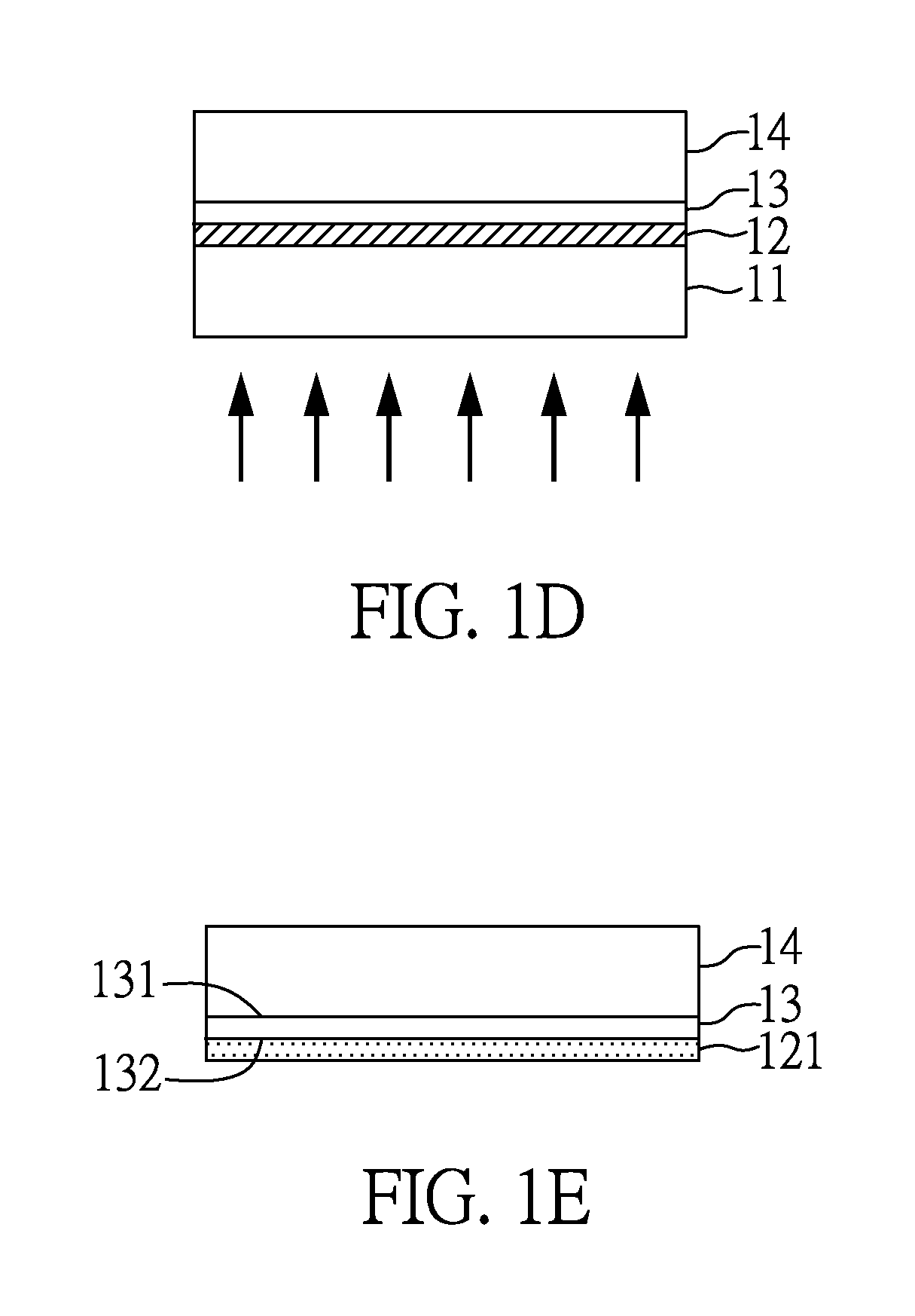
[0094]Hereinafter, the electronic apparatus and the method for manufacturing the same of one preferred embodiment of the present invention are illustrated in detail according to FIG. 1A to FIG. 1E.

[0095]First, as shown in FIG. 1A, a carrier 11 is provided, which can be a glass carrier, a quartz carrier, or a plastic carrier known in the art, and has a light transmittance larger than 30%. In the present embodiment, a glass substrate or a plastic substrate having high light transmittance is used.

[0096]Then, a debonding layer 12 is form...


PUM

PropertyMeasurementUnit
bending displacementaaaaaaaaaa
wavelengthaaaaaaaaaa
light transmittanceaaaaaaaaaa

Abstract

An electronic apparatus and a method for manufacturing the same are disclosed. The electronic device of the present invention comprises: a substrate with a first surface and a second surface; an electronic unit layer disposed on the first surface of the substrate; a residue layer disposed on the second surface of the substrate, wherein a material of the residue layer comprises: a compound containing at least one functional group selected from the group consisting of aryl, nitro and ketone.

Description

CROSS REFERENCE TO RELATED APPLICATION[0001]This application claims the benefits of the Taiwan Patent Application Serial Number 102120101 and 103106686, respectively filed on Jun. 6, 2013 and Feb. 27, 2014, the subject matter of which is incorporated herein by reference.BACKGROUND OF THE INVENTION[0002]1. Field of the Invention[0003]The present invention relates to an electronic apparatus and a method for manufacturing the same and, more particularly, to an electronic apparatus with a flexible substrate and a method for manufacturing the same.[0004]2. Description of Related Art[0005]As the demand for thin and light electronic devices, the glass substrate for the display panel is developed from a glass substrate having a thickness of about 0.4 mm toward a flexible substrate having a thickness of about 0.3 mm.[0006]However, when the flexible substrate is a thin glass substrate having a thickness of 0.3 mm or less or a plastic substrate, the rigidity thereof is not high enough for the ...

Claims


Application Information

Patent Timeline
Patent Type & Authority Patents(United States)
IPC IPC(8): B32B7/06G02F1/1333B32B38/10H01L51/00H05K3/00H05K1/03G02F1/13
CPCH05K3/007B32B7/06B32B38/10B32B2307/716B32B2310/08G02F1/1303Y10T428/31678H01L51/003H01L2251/5338H05K1/0306H05K1/0393H05K2203/016G02F1/133305H10K71/80H10K2102/311
Inventor TSAI, CHI-CHECHEN, YU-YAOHSU, PO-YUNWU, WEI-YEN
Owner INNOLUX CORP
Why Eureka
Try Eureka