Fingerprint sensing system with liveness detection
- Summary
- Abstract
- Description
- Claims
- Application Information
AI Technical Summary
Benefits of technology
Problems solved by technology
Method used
Image

Examples
first embodiment
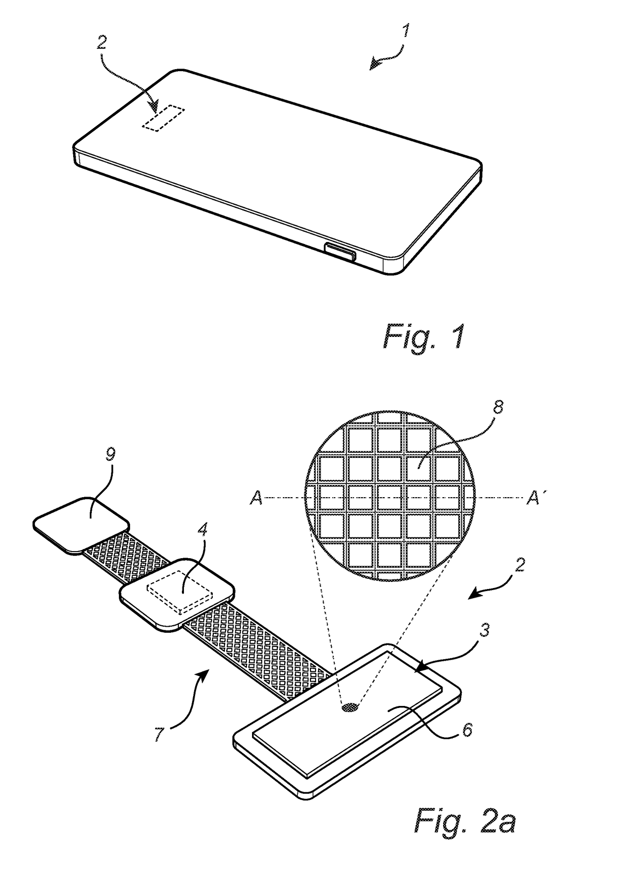
[0061]FIG. 2a schematically shows the fingerprint sensing system 2 comprised in the mobile phone 1 in FIG. 1. As can be seen in FIG. 2a, the fingerprint sensing system 2 comprises a fingerprint sensor 3 and an interface circuit 4. In the present exemplary embodiment, the fingerprint sensor 3 is shown to be coated with a dielectric structure in the form of a protective coating 6. Depending on the application, the protective coating 6 may have different properties. If the fingerprint sensor 3 is to be arranged under the cover glass of a mobile phone 1, then the protective coating 6 may be rather thin, since the cover glass will offer protection for the fingerprint sensor 3. In other applications, where the protective coating 6 is to be directly touched by the user's finger, the protective coating may be rather thick. For instance, the fingerprint sensor 3 may be overmolded by a suitable polymer used in the electronics packaging industry.
[0062]In the present exemplary embodiment, the f...
second embodiment
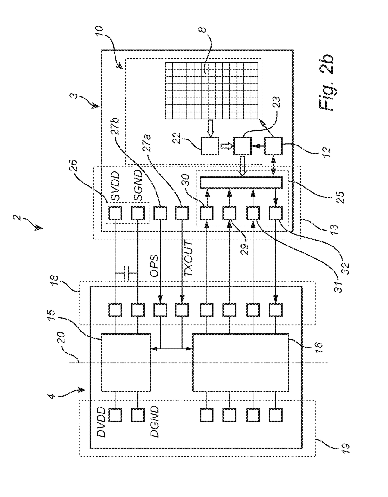
[0098]With reference to FIG. 5b, which is a simplified schematic block diagram of the fingerprint sensing system 2 in FIG. 5a, the fingerprint sensing system component 50 comprises a sensing arrangement 10, a sensing arrangement controller 12, supply circuitry 15, a level shifting circuitry 16, and a device connection interface 19. The sensing arrangement 10 and the sensing arrangement controller 12 are in a first voltage domain, and the device connection interface 19 and the ADC 23 are in a second voltage domain referenced to the device reference potential of the electronic device 1. The border between the first voltage domain and the second voltage domain is schematically indicated in FIG. 5b by the vertical dashed line 20 passing through the supply circuitry 15 and the level shifting circuitry 16.
[0099]The sensing arrangement 10 comprises the above-mentioned sensing elements 8 and sampling circuitry 22 for sampling sensing signals output by the sensing elements 8. In the example ...
PUM
 Abstract
Description
Claims
Application Information
 - R&D Engineer
- R&D Manager
- IP Professional
- Industry Leading Data Capabilities
- Powerful AI technology
- Patent DNA Extraction
Browse by: Latest US Patents, China's latest patents, Technical Efficacy Thesaurus, Application Domain, Technology Topic.
© 2024 PatSnap. All rights reserved.Legal|Privacy policy|Modern Slavery Act Transparency Statement|Sitemap